- 您现在的位置:买卖IC网 > PDF目录17104 > DC1112A (Linear Technology)BOARD DAC LTC2755-16 PDF资料下载
参数资料
| 型号: | DC1112A |
| 厂商: | Linear Technology |
| 文件页数: | 6/24页 |
| 文件大小: | 0K |
| 描述: | BOARD DAC LTC2755-16 |
| 软件下载: | QuikEval System |
| 设计资源: | DC1112A Design File DC1112A Schematic |
| 标准包装: | 1 |
| 系列: | QuikEval™, SoftSpan™ |
| DAC 的数量: | 4 |
| 位数: | 16 |
| 数据接口: | 并联 |
| 设置时间: | 2µs |
| DAC 型: | 电流 |
| 工作温度: | 0°C ~ 70°C |
| 已供物品: | 板 |
| 已用 IC / 零件: | LTC2755-16 |
| 相关产品: | DC590B-ND - BOARD DEMO USB SERIAL CONTROLLER LTC2755BIUP-16#TRPBF-ND - IC DAC 16BIT CUR OUT 64-QFN LTC2755BIUP-16#PBF-ND - IC DAC 16BIT CUR OUT 64-QFN LTC2755BCUP-16#TRPBF-ND - IC DAC 16BIT CUR OUT 64-QFN LTC2755BCUP-16#PBF-ND - IC DAC 16BIT CUR OUT 64-QFN LTC2755AIUP-16#TRPBF-ND - IC DAC 16BIT CUR OUT 64-QFN LTC2755AIUP-16#PBF-ND - IC DAC 16BIT CUR OUT 64-QFN LTC2755ACUP-16#TRPBF-ND - IC DAC 16BIT CUR OUT 64-QFN LTC2755ACUP-16#PBF-ND - IC DAC 16BIT CUR OUT 64-QFN |
LTC2755
14
2755f
Output Ranges
The LTC2755 is a quad current-output, parallel-input
precision multiplying DAC with selectable output ranges.
Rangescaneitherbeprogrammedinsoftwareformaximum
exibility, or hardwired through pin-strapping for greatest
ease of use. Two unipolar ranges are available (0V to 5V
and 0V to 10V), and four bipolar ranges (±2.5V, ±5V, ±10V
and –2.5V to 7.5V). These ranges are obtained when an
external precision 5V reference is used. When a reference
voltage of 2V is used, the ranges become: 0V to 2V, 0V
to 4V, ±1V, ±2V, ±4V and –1V to 3V. The output ranges are
linearly scaled for references other than 2V and 5V.
Digital Section
The LTC2755 has 4 internal registers for each DAC, a total
of 16 registers (see Block Diagram). Each DAC channel
has two sets of double-buffered registers—one set for
the data, and one set for the span (output range) of the
DAC. The double-buffered feature provides the capability
to simultaneously update the span and code, which al-
lows smooth voltage transitions when changing output
ranges. It also permits the simultaneous updating of
multiple DACs.
Each set of double-buffered registers comprises an input
register and a DAC register. The input registers are holding
buffers—when data is loaded into an input register via a
write operation, the DAC outputs are not affected.
The contents of a DAC register, on the other hand, di-
rectly control the DAC output voltage or output range.
The contents of the DAC registers are changed by copying
the contents of an input register into its associated DAC
register via an update operation.
Write and Update Operations
The data input register of the addressed DAC is loaded
directly from a 16-bit microprocessor bus by holding the
D/S pin low and pulsing the WR pin low (write operation).
The DAC register is loaded by pulsing the UPD pin high
(update operation), which copies the data held in the input
register into the DAC register. Note that updates always
include both data and span; but the DAC register values
will not change unless the associated input register values
have previously been changed via a write operation.
Loading the span input register is accomplished similarly,
holding the D/S pin high and pulsing the WR pin low. The
span and data register structures are the same except for
the number of parallel bits—the span registers have 3 bits,
while the data registers have 12, 14 or 16 bits.
To make both registers transparent for owthrough
mode, tie WR low and UPD high. However, this defeats
the deglitcher operation and output glitch impulse may
increase. The deglitcher is activated on the rising edge
of the UPD pin.
The interface also allows the use of the input and DAC
registers in a master-slave, or edge-triggered, congura-
tion. This mode of operation occurs when WR and UPD
are tied together and driven by a single clock signal. The
data bits are loaded into the input register on the falling
edge of the clock and then loaded into the DAC register
on the rising edge.
It is possible to control both data and span on one 16-bit
wide data bus by allowing span pins S2 to S0 to share
bus lines with the data LSBs (D2 to D0). No write or read
operation includes both span and data, so there cannot
be a conict.
The asynchronous clear pin resets all DACs to 0V in any
output range. CLR resets all data registers, while leaving
the span registers undisturbed.
OPERATION
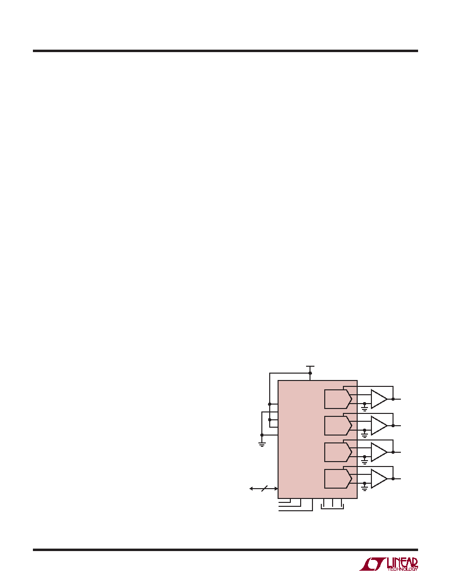
Figure 1. Using MSPAN to Congure the LTC2755 for Single-Span
Operation (±10V Range).
LTC2755-16
MSPAN
S2
S1
S0
D/S
2755 F01
WR UPD READ A2
DAC ADDRESS
A1 A0
DATA
I/O
VDD
DAC A
±10V
DAC B
DAC C
DAC D
16
–
+
–
+
–
+
–
+
相关PDF资料 |
PDF描述 |
|---|---|
| EEM36DRTH-S13 | CONN EDGECARD 72POS .156 EXTEND |
| EEM36DRKN-S13 | CONN EDGECARD 72POS .156 EXTEND |
| 0210390989 | CABLE JUMPER 1MM .051M 29POS |
| SCRH5D28-220 | INDUCTOR SMD 22UH 0.86A 10KHZ |
| EEM36DRKH-S13 | CONN EDGECARD 72POS .156 EXTEND |
相关代理商/技术参数 |
参数描述 |
|---|---|
| DC1112H | 制造商:未知厂家 制造商全称:未知厂家 功能描述:D_1112H Series, Thin Type InGaN/SiC SMT LED |
| DC1112H-TR | 功能描述:LED BLUISH-GREEN 0805 SMD RoHS:是 类别:光电元件 >> LED - 1112H 标准包装:500 系列:Screenmaster® 颜色:琥珀 Millicandela 等级:2260mcd 正向电压:2.1V 电流 - 测试:20mA 波长 - 主:590nm 波长 - 峰值:- 视角:- 透镜类型:散射,有色 透镜样式/尺寸:圆顶椭圆,5.1mm x 3.7mm 封装/外壳:径向 尺寸/尺寸:- 高度:7.00mm 安装类型:通孔 包装:散装 在特定电流下的光通量 - 测试:- |
| DC1113B | 制造商:Intel 功能描述:113B |
| DC1113F-TR | 功能描述:LED BLUE-GREEN RIGHT ANGLE SMD RoHS:是 类别:光电元件 >> LED - 1113F 标准包装:500 系列:Screenmaster® 颜色:琥珀 Millicandela 等级:2260mcd 正向电压:2.1V 电流 - 测试:20mA 波长 - 主:590nm 波长 - 峰值:- 视角:- 透镜类型:散射,有色 透镜样式/尺寸:圆顶椭圆,5.1mm x 3.7mm 封装/外壳:径向 尺寸/尺寸:- 高度:7.00mm 安装类型:通孔 包装:散装 在特定电流下的光通量 - 测试:- |
| DC111492 | 制造商:ITT Interconnect Solutions 功能描述:DC111492 - Bulk |
发布紧急采购,3分钟左右您将得到回复。