- 您现在的位置:买卖IC网 > PDF目录19029 > DC1525A-A (Linear Technology)BOARD DEMO 125MSPS LTC2175-14 PDF资料下载
参数资料
| 型号: | DC1525A-A |
| 厂商: | Linear Technology |
| 文件页数: | 18/34页 |
| 文件大小: | 0K |
| 描述: | BOARD DEMO 125MSPS LTC2175-14 |
| 软件下载: | QuikEval II System |
| 设计资源: | DC1525A Design Files |
| 标准包装: | 1 |
| 系列: | * |
| 相关产品: | DC1371A-ND - BOARD USB DATA ACQUISITION HS |
第1页第2页第3页第4页第5页第6页第7页第8页第9页第10页第11页第12页第13页第14页第15页第16页第17页当前第18页第19页第20页第21页第22页第23页第24页第25页第26页第27页第28页第29页第30页第31页第32页第33页第34页
25
21754314fa
LTC2175-14/
LTC2174-14/LTC2173-14
applicaTions inForMaTion
mode. Recovering from nap mode requires at least 100
clock cycles. If the application demands very accurate DC
settling then an additional 50s should be allowed so the
on-chip references can settle from the slight temperature
shift caused by the change in supply current as the A/D
leaves nap mode. Nap mode is enabled by mode control
register A1 in the serial programming mode.
DEVICE PROGRAMMING MODES
The operating modes of the LTC2175-14/LTC2174-14/
LTC2173-14 can be programmed by either a parallel in-
terface or a simple serial interface. The serial interface has
more flexibility and can program all available modes. The
parallel interface is more limited and can only program
some of the more commonly used modes.
Parallel Programming Mode
To use the parallel programming mode, PAR/SER should
be tied to VDD. The CS, SCK, SDI and SDO pins are binary
logic inputs that set certain operating modes. These pins
can be tied to VDD or ground, or driven by 1.8V, 2.5V, or
3.3V CMOS logic. When used as an input, SDO should
be driven through a 1k series resistor. Table 3 shows the
modes set by CS, SCK, SDI and SDO.
Serial Programming Mode
To use the serial programming mode, PAR/SER should be
tied to ground. The CS, SCK, SDI and SDO pins become a
serialinterfacethatprogramtheA/Dmodecontrolregisters.
Data is written to a register with a 16-bit serial word. Data
can also be read back from a register to verify its contents.
Serial data transfer starts when CS is taken low. The data
on the SDI pin is latched at the first 16 rising edges of
SCK. Any SCK rising edges after the first 16 are ignored.
The data transfer ends when CS is taken high again.
The first bit of the 16-bit input word is the R/W bit. The
next seven bits are the address of the register (A6:A0).
The final eight bits are the register data (D7:D0).
If the R/W bit is low, the serial data (D7:D0) will be writ-
ten to the register set by the address bits (A6:A0). If the
R/W bit is high, data in the register set by the address bits
(A6:A0) will be read back on the SDO pin (see the Timing
Diagrams sections). During a read back command the
register is not updated and data on SDI is ignored.
The SDO pin is an open-drain output that pulls to ground
with a 200 impedance. If register data is read back
through SDO, an external 2k pull-up resistor is required.
If serial data is only written and read back is not needed,
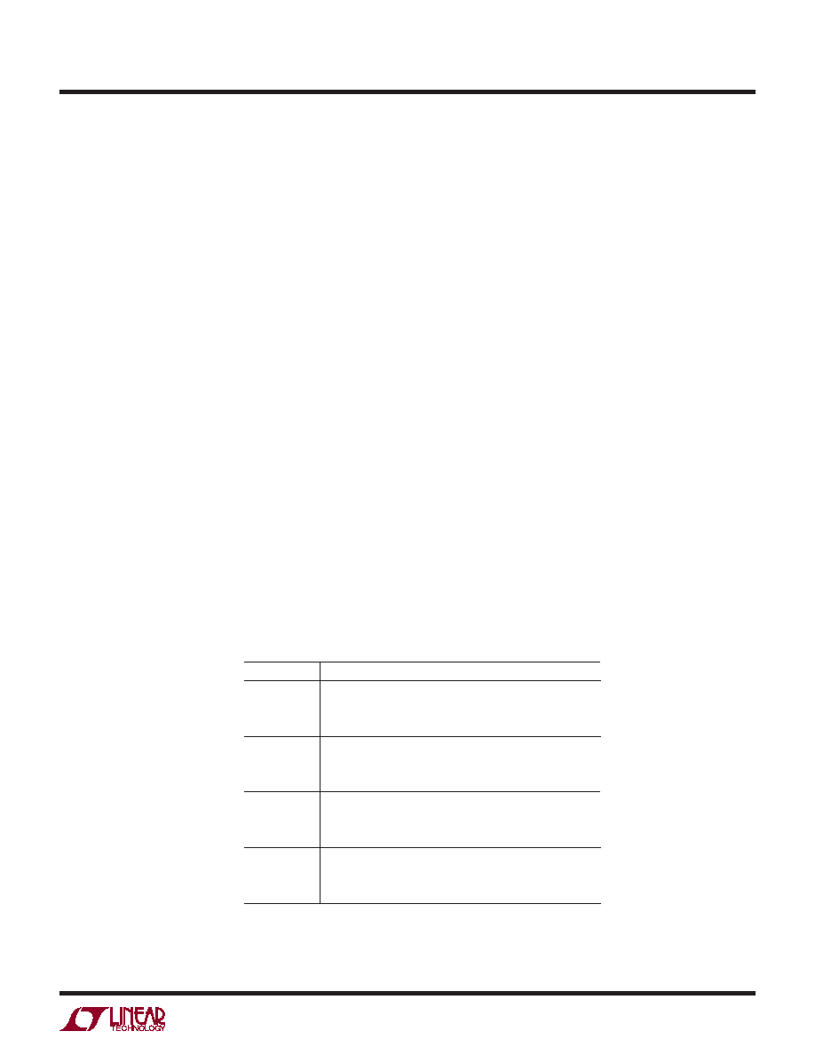
Table 3. Parallel Programming Mode Control Bits (PAR/SER = VDD)
Pin
DESCRIPTION
CS
2-Lane / 1-Lane Selection Bit
0 = 2-Lane, 16-Bit Serialization Output Mode
1 = 1-Lane, 14-Bit Serialization Output Mode
SCK
LVDS Current Selection Bit
0 = 3.5mA LVDS Current Mode
1 = 1.75mA LVDS Current Mode
SDI
Power Down Control Bit
0 = Normal Operation
1 = Sleep Mode
SDO
Internal Termination Selection Bit
0 = Internal Termination Disabled
1 = Internal Termination Enabled
相关PDF资料 |
PDF描述 |
|---|---|
| 48ESB | LAMP INCAND T-2 TELE SLIDE 48V |
| CQM1-TC201 | 4 LOOP THERMOCPLE IN NPN OUT |
| 35A1 | LAMP INCAND T-2 TELE SLIDE 35V |
| 24B1 | LAMP INCAND T-2 TELE SLIDE 24V |
| 8098 | LAMP INCAND 3MM STD BI-PIN 14V |
相关代理商/技术参数 |
参数描述 |
|---|---|
| DC1525A-B | 功能描述:BOARD DEMO 105MSPS LTC2174-14 RoHS:是 类别:未定义的类别 >> 其它 系列:* 标准包装:1 系列:* 其它名称:MS305720A |
| DC1525A-C | 功能描述:BOARD DEMO 80MSPS LTC2173-14 RoHS:是 类别:未定义的类别 >> 其它 系列:* 标准包装:1 系列:* 其它名称:MS305720A |
| DC1525A-D | 功能描述:BOARD DEMO 65MSPS LTC2172-14 RoHS:是 类别:未定义的类别 >> 其它 系列:* 标准包装:1 系列:* 其它名称:MS305720A |
| DC1525A-E | 功能描述:BOARD DEMO 40MSPS LTC2171-14 RoHS:是 类别:未定义的类别 >> 其它 系列:* 标准包装:1 系列:* 其它名称:MS305720A |
| DC1525A-F | 功能描述:BOARD DEMO 25MSPS LTC2170-14 RoHS:是 类别:未定义的类别 >> 其它 系列:* 标准包装:1 系列:* 其它名称:MS305720A |
发布紧急采购,3分钟左右您将得到回复。