- 您现在的位置:买卖IC网 > PDF目录19029 > DC1525A-B (Linear Technology)BOARD DEMO 105MSPS LTC2174-14 PDF资料下载
参数资料
| 型号: | DC1525A-B |
| 厂商: | Linear Technology |
| 文件页数: | 19/34页 |
| 文件大小: | 0K |
| 描述: | BOARD DEMO 105MSPS LTC2174-14 |
| 软件下载: | QuikEval II System |
| 设计资源: | DC1525A Design Files |
| 标准包装: | 1 |
| 系列: | * |
| 相关产品: | DC1371A-ND - BOARD USB DATA ACQUISITION HS |
第1页第2页第3页第4页第5页第6页第7页第8页第9页第10页第11页第12页第13页第14页第15页第16页第17页第18页当前第19页第20页第21页第22页第23页第24页第25页第26页第27页第28页第29页第30页第31页第32页第33页第34页
LTC2175-14/
LTC2174-14/LTC2173-14
26
21754314fa
applicaTions inForMaTion
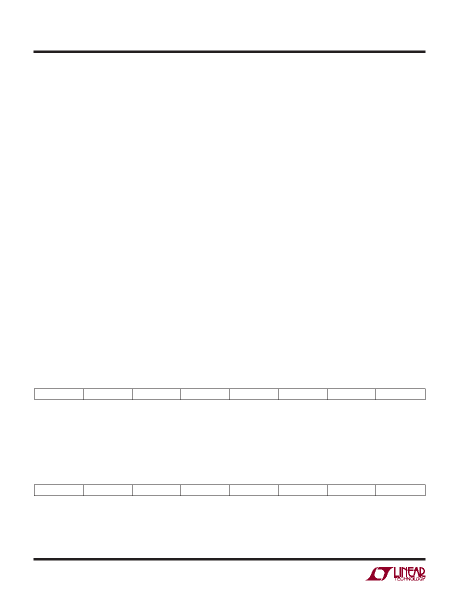
Table 4. Serial Programming Mode Register Map (PAR/SER = GND)
REGISTER A0: RESET REGISTER (ADDRESS 00h)
D7
D6
D5
D4
D3
D2
D1
D0
RESET
X
Bit 7
RESET
Software Reset Bit
0 = Not Used
1 = Software Reset. All Mode Control Registers are Reset to 00h. The ADC is Momentarily Placed in SLEEP Mode.
This Bit is Automatically Set Back to Zero at the End of the SPI Write Command.
The Reset Register is Write Only.
Bits 6-0
Unused, Don’t Care Bits.
REGISTER A1: FORMAT AND POWER-DOWN REGISTER (ADDRESS 01h)
D7
D6
D5
D4
D3
D2
D1
D0
DCSOFF
RAND
TWOSCOMP
SLEEP
NAP_4
NAP_3
NAP_2
NAP_1
Bit 7
DCSOFF
Clock Duty Cycle Stabilizer Bit
0 = Clock Duty Cycle Stabilizer On
1 = Clock Duty Cycle Stabilizer Off. This is Not Recommended.
Bit 6
RAND
Data Output Randomizer Mode Control Bit
0 = Data Output Randomizer Mode Off
1 = Data Output Randomizer Mode On
then SDO can be left floating and no pull-up resistor is
needed.Table4showsamapofthemodecontrolregisters.
Software Reset
If serial programming is used, the mode control registers
shouldbeprogrammedassoonaspossibleafterthepower
supplies turn on and are stable. The first serial command
must be a software reset which will reset all register data
bits to logic 0. To perform a software reset, bit D7 in the
reset register is written with a logic 1. After the reset SPI
write command is complete, bit D7 is automatically set
back to zero.
GROUNDING AND BYPASSING
The LTC2175-14/LTC2174-14/LTC2173-14 requires a
printed circuit board with a clean unbroken ground plane.
A multilayer board with an internal ground plane in the
first layer beneath the ADC is recommended. Layout for
the printed circuit board should ensure that digital and
analog signal lines are separated as much as possible. In
particular, care should be taken not to run any digital track
alongside an analog signal track or underneath the ADC.
High quality ceramic bypass capacitors should be used
at the VDD, OVDD, VCM, VREF, REFH and REFL pins. By-
pass capacitors must be located as close to the pins as
possible. Of particular importance is the 0.1F capacitor
between REFH and REFL. This capacitor should be on the
same side of the circuit board as the A/D, and as close to
the device as possible (1.5mm or less). Size 0402 ceramic
capacitors are recommended. The larger 2.2F capacitor
between REFH and REFL can be somewhat further away.
Thetracesconnectingthepinsandbypasscapacitorsmust
be kept short and should be made as wide as possible.
The analog inputs, encode signals, and digital outputs
should not be routed next to each other. Ground fill and
grounded vias should be used as barriers to isolate these
signals from each other.
HEAT TRANSFER
MostoftheheatgeneratedbytheLTC2175-14/LTC2174-14/
LTC2173-14istransferredfromthediethroughthebottom-
sideExposedPadandpackageleadsontotheprintedcircuit
board. For good electrical and thermal performance, the
Exposed Pad must be soldered to a large grounded pad
on the PC board. This pad should be connected to the
internal ground planes by an array of vias.
相关PDF资料 |
PDF描述 |
|---|---|
| 407 | LAMP INCAND G-4.5 MINI FLSH 4.9V |
| 60PSB | LAMP INCAND T-2 TELE SLIDE 60V |
| 204-0131-200 | CAP MINI DIMMER PANEL IND RED |
| 7234 | LAMP INCAND 3MM STD MIDGET 5V |
| 8099SBP | LAMP INCAND 3MM SPEC BI-PIN 18V |
相关代理商/技术参数 |
参数描述 |
|---|---|
| DC1525A-C | 功能描述:BOARD DEMO 80MSPS LTC2173-14 RoHS:是 类别:未定义的类别 >> 其它 系列:* 标准包装:1 系列:* 其它名称:MS305720A |
| DC1525A-D | 功能描述:BOARD DEMO 65MSPS LTC2172-14 RoHS:是 类别:未定义的类别 >> 其它 系列:* 标准包装:1 系列:* 其它名称:MS305720A |
| DC1525A-E | 功能描述:BOARD DEMO 40MSPS LTC2171-14 RoHS:是 类别:未定义的类别 >> 其它 系列:* 标准包装:1 系列:* 其它名称:MS305720A |
| DC1525A-F | 功能描述:BOARD DEMO 25MSPS LTC2170-14 RoHS:是 类别:未定义的类别 >> 其它 系列:* 标准包装:1 系列:* 其它名称:MS305720A |
| DC1525A-G | 功能描述:BOARD DEMO 125MSPS LTC2175-12 RoHS:是 类别:未定义的类别 >> 其它 系列:* 标准包装:1 系列:* 其它名称:MS305720A |
发布紧急采购,3分钟左右您将得到回复。