- 您现在的位置:买卖IC网 > PDF目录19027 > DC1525A-F (Linear Technology)BOARD DEMO 25MSPS LTC2170-14 PDF资料下载
参数资料
| 型号: | DC1525A-F |
| 厂商: | Linear Technology |
| 文件页数: | 19/34页 |
| 文件大小: | 0K |
| 描述: | BOARD DEMO 25MSPS LTC2170-14 |
| 软件下载: | QuikEval II System |
| 设计资源: | DC1525A Design Files |
| 标准包装: | 1 |
| 系列: | * |
| 相关产品: | DC1371A-ND - BOARD USB DATA ACQUISITION HS |
第1页第2页第3页第4页第5页第6页第7页第8页第9页第10页第11页第12页第13页第14页第15页第16页第17页第18页当前第19页第20页第21页第22页第23页第24页第25页第26页第27页第28页第29页第30页第31页第32页第33页第34页
LTC2172-14/
LTC2171-14/LTC2170-14
26
21721014fb
applicaTions inForMaTion
The first bit of the 16-bit input word is the R/W bit. The
next seven bits are the address of the register (A6:A0).
The final eight bits are the register data (D7:D0).
If the R/W bit is low, the serial data (D7:D0) will be
written to the register set by the address bits (A6:A0).
If the R/W bit is high, data in the register set by the
address bits (A6:A0) will be read back on the SDO pin
(see the Timing Diagrams section). During a readback
command the register is not updated and data on SDI
is ignored.
The SDO pin is an open-drain output that pulls to ground
with a 200 impedance. If register data is read back
through SDO, an external 2k pull-up resistor is required.
If serial data is only written and readback is not needed,
then SDO can be left floating and no pull-up resistor is
needed.Table4showsamapofthemodecontrolregisters.
Software Reset
If serial programming is used, the mode control registers
shouldbeprogrammedassoonaspossibleafterthepower
supplies turn on and are stable. The first serial command
must be a software reset which will reset all register data
bits to logic 0. To perform a software reset, bit D7 in the
reset register is written with a logic 1. After the reset SPI
write command is complete, bit D7 is automatically set
back to zero.
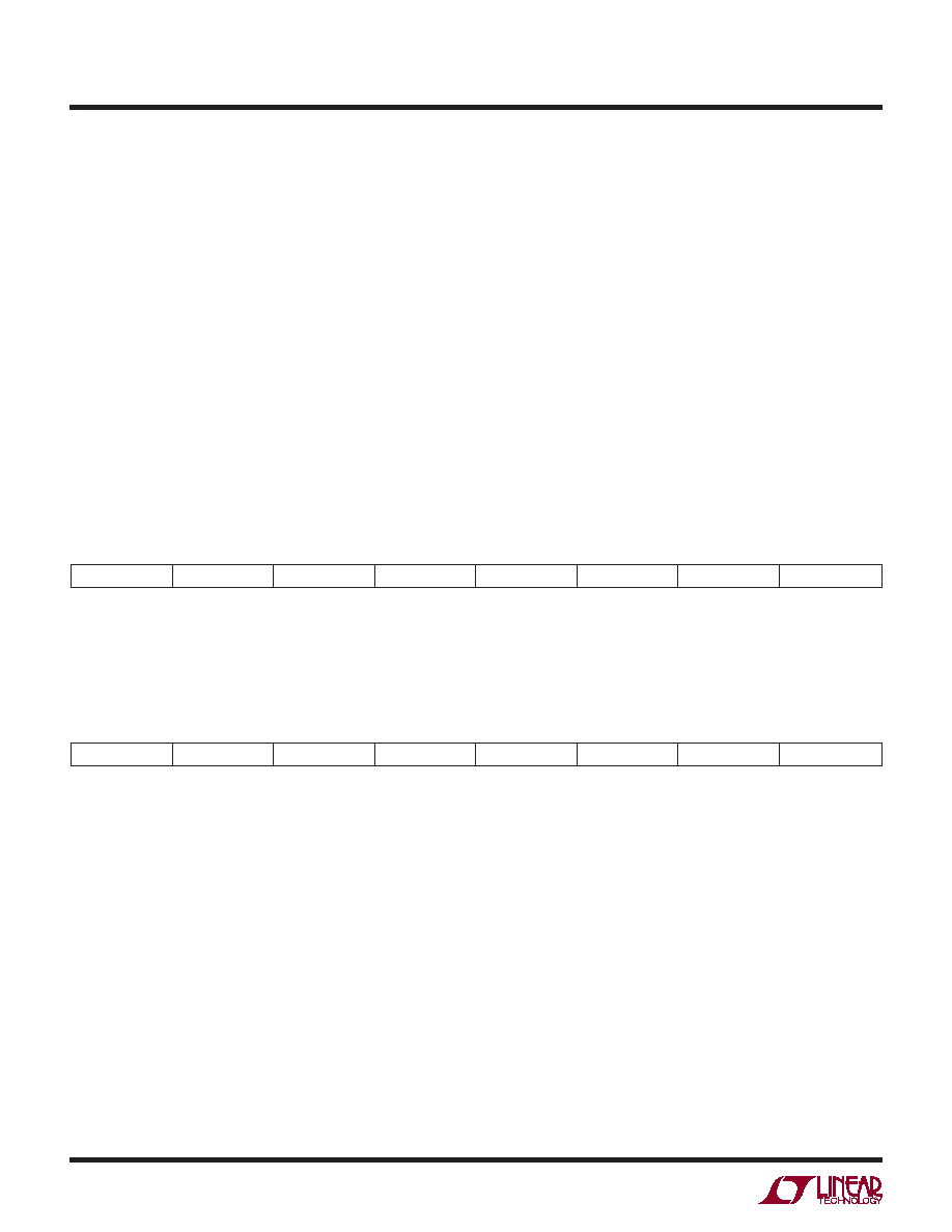
Table 4. Serial Programming Mode Register Map (PAR/SER = GND)
REGISTER A0: RESET REGISTER (ADDRESS 00h)
D7
D6
D5
D4
D3
D2
D1
D0
RESET
X
Bit 7
RESET
Software Reset Bit
0 = Not Used
1 = Software Reset. All Mode Control Registers Are Reset to 00h. The ADC is momentarily placed in SLEEP mode. This bit is
automatically set back to zero after the reset is complete at the end of the SPI write command. The reset register is write only.
Bits 6-0
Unused, Don’t Care Bits.
REGISTER A1: POWER-DOWN REGISTER (ADDRESS 01h)
D7
D6
D5
D4
D3
D2
D1
D0
DCSOFF
RAND
TWOSCOMP
SLEEP
NAP_4
NAP_3
NAP_2
NAP_1
Bit 7
DCSOFF
Clock Duty Cycle Stabilizer Bit
0 = Clock Duty Cycle Stabilizer On
1 = Clock Duty Cycle Stabilizer Off. This is Not Recommended.
Bit 6
RAND
Data Output Randomizer Mode Control Bit
0 = Data Output Randomizer Mode Off
1 = Data Output Randomizer Mode On
Bit 5
TWOSCOMP
Two’s Complement Mode Control Bit
0 = Offset Binary Data Format
1 = Two’s Complement Data Format
Bits 4-0
SLEEP:NAP_4:NAP_1
Sleep/Nap Mode Control Bits
00000 = Normal Operation
0XXX1 = Channel 1 in Nap Mode
0XX1X = Channel 2 in Nap Mode
0X1XX = Channel 3 in Nap Mode
01XXX = Channel 4 in Nap Mode
1XXXX = Sleep Mode. All Channels Are Disabled
Note: Any Combination of Channels Can Be Placed in Nap Mode.
相关PDF资料 |
PDF描述 |
|---|---|
| 10S6-230V | LAMP INCAND S6 CNDLBRA SCRW 230V |
| 6180 | LAMP INCAND 3MM STD MIDGET 5V |
| 714 | LAMP INCAND 3MM STD MIDGET 5V |
| 120PSB | LAMP INCAND T-2 TELE SLIDE 120V |
| 6152 | LAMP INCAND 3MM WIRE TERM 5V |
相关代理商/技术参数 |
参数描述 |
|---|---|
| DC1525A-G | 功能描述:BOARD DEMO 125MSPS LTC2175-12 RoHS:是 类别:未定义的类别 >> 其它 系列:* 标准包装:1 系列:* 其它名称:MS305720A |
| DC1525A-H | 功能描述:BOARD DEMO 105MSPS LTC2174-12 RoHS:是 类别:未定义的类别 >> 其它 系列:* 标准包装:1 系列:* 其它名称:MS305720A |
| DC1525A-I | 功能描述:BOARD DEMO 80MSPS LTC2173-12 RoHS:是 类别:未定义的类别 >> 其它 系列:* 标准包装:1 系列:* 其它名称:MS305720A |
| DC1525A-J | 功能描述:BOARD DEMO 65MSPS LTC2172-12 RoHS:是 类别:未定义的类别 >> 其它 系列:* 标准包装:1 系列:* 其它名称:MS305720A |
| DC1525A-K | 功能描述:BOARD DEMO 40MSPS LTC2171-12 RoHS:是 类别:未定义的类别 >> 其它 系列:* 标准包装:1 系列:* 其它名称:MS305720A |
发布紧急采购,3分钟左右您将得到回复。