- 您现在的位置:买卖IC网 > PDF目录17032 > DC1813A-C (Linear Technology)BOARD SAR ADC LTC2367-16 PDF资料下载
参数资料
| 型号: | DC1813A-C |
| 厂商: | Linear Technology |
| 文件页数: | 11/28页 |
| 文件大小: | 0K |
| 描述: | BOARD SAR ADC LTC2367-16 |
| 软件下载: | QuikEval II System |
| 设计资源: | DC1813A Design File DC1813A Schematic |
| 标准包装: | 1 |
| 系列: | QuikEval-II™ |
| ADC 的数量: | 1 |
| 位数: | 16 |
| 采样率(每秒): | 500k |
| 数据接口: | 串行,SPI? |
| 输入范围: | 0 ~ VREF |
| 在以下条件下的电源(标准): | 6.75mW @ 500kSPS |
| 工作温度: | 0°C ~ 70°C |
| 已用 IC / 零件: | LTC2367-16 |
| 已供物品: | 板 |
| 相关产品: | LTC2367HMS-16#TRPBF-ND - IC ADC 16BIT SPI/SRL 500K 16MSOP LTC2367HMS-16#PBF-ND - IC ADC 16BIT SPI/SRL 500K 16MSOP LTC2367CMS-16#TRPBF-ND - IC ADC 16BIT SPI/SRL 500K 16MSOP LTC2367CDE-16#TRPBF-ND - IC ADC 16BIT SPI/SRL 500K 16-DFN LTC2367CDE-16#PBF-ND - IC ADC 16BIT SPI/SRL 500K 16-DFN LTC2367IDE-16#TRPBF-ND - IC ADC 16BIT SPI/SRL 500K 16-DFN LTC2367IDE-16#PBF-ND - IC ADC 16BIT SPI/SRL 500K 16-DFN LTC2367IMS-16#TRPBF-ND - IC ADC 16BIT SPI/SRL 500K 16MSOP LTC2367IMS-16#PBF-ND - IC ADC 16BIT SPI/SRL 500K 16MSOP LTC2367CMS-16#PBF-ND - IC ADC 16BIT SPI/SRL 500K 16MSOP 更多... |
第1页第2页第3页第4页第5页第6页第7页第8页第9页第10页当前第11页第12页第13页第14页第15页第16页第17页第18页第19页第20页第21页第22页第23页第24页第25页第26页第27页第28页
LT6202/LT6203/LT6204
19
620234fd
APPLICATIONS INFORMATION
Input Protection
There are back-to-back diodes, D1 and D2, across the
+ and – inputs of these amplifiers to limit the differential
input voltage to ±0.7V. The inputs of the LT6202/LT6203/
LT6304 do not have internal resistors in series with the
input transistors. This technique is often used to protect
the input devices from over voltage that causes excessive
currents to flow. The addition of these resistors would
significantly degrade the low noise voltage of these ampli-
fiers.Forinstance,a100Ωresistorinserieswitheachinput
would generate 1.8nV/√Hz of noise, and the total amplifier
noise voltage would rise from 1.9nV/√Hz to 2.6nV/√Hz.
Once the input differential voltage exceeds ±0.7V, steady
state current conducted though the protection diodes
should be limited to ±40mA. This implies 25Ω of protec-
tion resistance per volt of continuous overdrive beyond
±0.7V. The input diodes are rugged enough to handle
transient currents due to amplifier slew rate overdrive or
momentary clipping without these resistors.
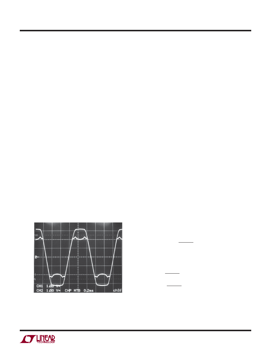
Figure 2 shows the input and output waveforms of the
amplifier driven into clipping while connected in a gain
of AV = 1. When the input signal goes sufficiently beyond
the power supply rails, the input transistors will saturate.
When saturation occurs, the amplifier loses a stage of
phase inversion and the output tries to change states.
Diodes D1 and D2 forward bias and hold the output within
OV
Figure 2. VS = ±2.5V, AV = 1 with Large Overdrive
a diode drop of the input signal. In this photo, the input
signal generator is clipping at ±35mA, and the output
transistors supply this generator current through the
protection diodes.
With the amplifier connected in a gain of AV ≥ 2, the output
can invert with very heavy input overdrive. To avoid this
inversion, limit the input overdrive to 0.5V beyond the
power supply rails.
ESD
The LT6202/LT6203/LT6204 have reverse-biased ESD
protection diodes on all inputs and outputs as shown in
Figure 1. If these pins are forced beyond either supply,
unlimited current will flow through these diodes. If the
current is transient and limited to one hundred milliamps
or less, no damage to the device will occur.
Noise
The noise voltage of the LT6202/LT6203/LT6204 is equiva-
lent to that of a 225Ω resistor, and for the lowest possible
noise it is desirable to keep the source and feedback re-
sistance at or below this value, i.e. RS + RG||RFB ≤ 225Ω.
With RS + RG||RFB = 225Ω the total noise of the amplifier
is: en = √(1.9nV)2+(1.9nV)2 = 2.7nV. Below this resis-
tance value, the amplifier dominates the noise, but in the
resistanceregionbetween225Ωandapproximately10kΩ,
the noise is dominated by the resistor thermal noise. As
the total resistance is further increased, beyond 10k, the
noise current multiplied by the total resistance eventually
dominates the noise.
The product of en √ISUPPLY is an interesting way to gauge
lownoiseamplifiers.Manylownoiseamplifierswithlowen
have high ISUPPLY current. In applications that require low
noise with the lowest possible supply current, this product
can prove to be enlightening. The LT6202/LT6203/LT6204
have an en, √ISUPPLY product of 3.2 per amplifier, yet it is
commontoseeamplifierswithsimilarnoisespecifications
have an en √ISUPPLY product of 4.7 to 13.5.
For a complete discussion of amplifier noise, see the
LT1028 data sheet.
相关PDF资料 |
PDF描述 |
|---|---|
| ADR433ARMZ-REEL7 | IC VREF SERIES PREC 3V 8-MSOP |
| ECE-V1CA471UP | CAP ALUM 470UF 16V 20% SMD |
| GEM31DCAN | CONN EDGECARD 62POS R/A .156 SLD |
| DC1813A-H | BOARD SAR ADC LTC2364-18 |
| FPF2312MPX | IC LOAD SW 2CH ADJ CURR 8-MLP |
相关代理商/技术参数 |
参数描述 |
|---|---|
| DC1813A-D | 功能描述:BOARD SAR ADC LTC2364-16 RoHS:是 类别:编程器,开发系统 >> 评估板 - 模数转换器 (ADC) 系列:QuikEval-II™ 产品培训模块:Obsolescence Mitigation Program 标准包装:1 系列:- ADC 的数量:1 位数:12 采样率(每秒):94.4k 数据接口:USB 输入范围:±VREF/2 在以下条件下的电源(标准):- 工作温度:-40°C ~ 85°C 已用 IC / 零件:MAX11645 已供物品:板,软件 |
| DC1813A-E | 功能描述:BOARD SAR ADC LTC2369-18 RoHS:是 类别:编程器,开发系统 >> 评估板 - 模数转换器 (ADC) 系列:QuikEval-II™ 产品培训模块:Obsolescence Mitigation Program 标准包装:1 系列:- ADC 的数量:1 位数:12 采样率(每秒):94.4k 数据接口:USB 输入范围:±VREF/2 在以下条件下的电源(标准):- 工作温度:-40°C ~ 85°C 已用 IC / 零件:MAX11645 已供物品:板,软件 |
| DC1813A-F | 功能描述:BOARD SAR ADC LTC2368-18 RoHS:是 类别:编程器,开发系统 >> 评估板 - 模数转换器 (ADC) 系列:QuikEval-II™ 产品培训模块:Obsolescence Mitigation Program 标准包装:1 系列:- ADC 的数量:1 位数:12 采样率(每秒):94.4k 数据接口:USB 输入范围:±VREF/2 在以下条件下的电源(标准):- 工作温度:-40°C ~ 85°C 已用 IC / 零件:MAX11645 已供物品:板,软件 |
| DC1813A-G | 功能描述:BOARD SAR ADC LTC2367-18 RoHS:是 类别:编程器,开发系统 >> 评估板 - 模数转换器 (ADC) 系列:QuikEval-II™ 产品培训模块:Obsolescence Mitigation Program 标准包装:1 系列:- ADC 的数量:1 位数:12 采样率(每秒):94.4k 数据接口:USB 输入范围:±VREF/2 在以下条件下的电源(标准):- 工作温度:-40°C ~ 85°C 已用 IC / 零件:MAX11645 已供物品:板,软件 |
| DC1813A-H | 功能描述:BOARD SAR ADC LTC2364-18 RoHS:是 类别:编程器,开发系统 >> 评估板 - 模数转换器 (ADC) 系列:QuikEval-II™ 产品培训模块:Obsolescence Mitigation Program 标准包装:1 系列:- ADC 的数量:1 位数:12 采样率(每秒):94.4k 数据接口:USB 输入范围:±VREF/2 在以下条件下的电源(标准):- 工作温度:-40°C ~ 85°C 已用 IC / 零件:MAX11645 已供物品:板,软件 |
发布紧急采购,3分钟左右您将得到回复。