- 您现在的位置:买卖IC网 > PDF目录17032 > DC1826A-A (Linear Technology)BOARD SAR ADC LTC2389-18 PDF资料下载
参数资料
| 型号: | DC1826A-A |
| 厂商: | Linear Technology |
| 文件页数: | 2/26页 |
| 文件大小: | 0K |
| 描述: | BOARD SAR ADC LTC2389-18 |
| 软件下载: | QuikEval II System |
| 设计资源: | DC1826A Schematic DC1826A Design Files |
| 标准包装: | 1 |
| 系列: | QuikEval-II™ |
| ADC 的数量: | 1 |
| 位数: | 18 |
| 采样率(每秒): | 2.5M |
| 数据接口: | 串行,并联 |
| 输入范围: | ±4.096 V |
| 在以下条件下的电源(标准): | 162.5mW @ 2.5MSPS |
| 工作温度: | 0°C ~ 70°C |
| 已用 IC / 零件: | LTC2389-18 |
| 已供物品: | 板 |
| 相关产品: | LTC2389IUK-18#TRPBF-ND - IC ADC 18BIT PAR/SRL 2.5M 48-QFN LTC2389HLX-18#PBF-ND - IC ADC 18BIT PAR/SRL 2.5M 48LQFP LTC2389CUK-18#TRPBF-ND - IC ADC 18BIT PAR/SRL 2.5M 48-QFN LTC2389CUK-18#PBF-ND - IC ADC 18BIT PAR/SRL 2.5M 48-QFN LTC2389CLX-18#PBF-ND - IC ADC 18BIT PAR/SRL 2.5M 48LQFP LTC2389IUK-18#PBF-ND - IC ADC SAR 48QFN LTC2389ILX-18#PBF-ND - IC ADC SAR 48LQFP DC718C-ND - DEMO QUIKEVAL-II DATA |
LT6200/LT6200-5
LT6200-10/LT6201
10
62001ff
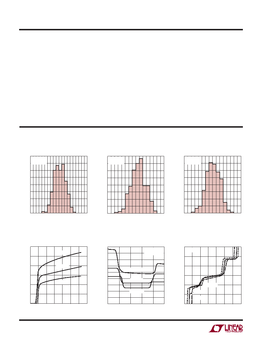
VOS Distribution, VCM = V+/2
INPUT OFFSET VOLTAGE (V)
–1000
NUMBER
OF
UNITS
80
70
60
50
40
30
20
10
0
600
6200 G01
–600
–200
200
1000
VS = 5V, 0V
SO-8
INPUT OFFSET VOLTAGE (V)
–1600–1200
NUMBER
OF
UNITS
40
60
1600
6200 G02
20
0
–800 –400 0
400 800 1200
80
30
50
10
70
VS = 5V, 0V
SO-8
INPUT OFFSET VOLTAGE (V)
–1600–1200
NUMBER
OF
UNITS
40
60
1600
6200 G03
20
0
–800 –400 0
400 800 1200
80
30
50
10
70
VS = 5V, 0V
SO-8
VOS Distribution, VCM = V+
VOS Distribution, VCM = V–
Note 3: A heat sink may be required to keep the junction temperature
below the absolute maximum rating when the output is shorted
indefinitely. The LT6201 in the DD package is limited by power dissipation
to VS ≤ 5V, 0V over the commercial temperature range only.
Note 4: The LT6200C/LT6200I and LT6201C/LT6201I are guaranteed functional
over the temperature range of –40°C and 85°C (LT6201DD excluded).
Note 5: The LT6200C/LT6201C are guaranteed to meet specified
performance from 0°C to 70°C. The LT6200C/LT6201C are designed,
characterized and expected to meet specified performance from –40°C
to 85°C, but are not tested or QA sampled at these temperatures. The
LT6200I is guaranteed to meet specified performance from –40°C to 85°C.
Note 6: Minimum supply voltage is guaranteed by power supply rejection
ratio test.
Note 7: Output voltage swings are measured between the output and
power supply rails.
Note 8: This parameter is not 100% tested.
Note 9: Full-power bandwidth is calculated from the slew rate:
FPBW = SR/2πVP
Note 10: Thermal resistance varies depending upon the amount of PC board
metal attached to the V– pin of the device.
θJA is specified for a certain
amount of 2oz copper metal trace connecting to the V– pin as described in
the thermal resistance tables in the Application Information section.
Note 11: Matching parameters on the LT6201 are the difference between
the two amplifiers. CMRR and PSRR match are defined as follows: CMRR
and PSRR are measured in V/V on the identical amplifiers. The difference
is calculated in V/V. The result is converted to dB.
Note 12: There are reverse biased ESD diodes on all inputs and outputs, as
shown in Figure 1. If these pins are forced beyond either supply, unlimited
current will flow through these diodes. If the current is transient in nature
and limited to less than 30mA, no damage to the device will occur.
Supply Current vs Supply Voltage
Offset Voltage
vs Input Common Mode Voltage
Input Bias Current
vs Common Mode Voltage
TOTAL SUPPLY VOLTAGE (V)
0
SUPPLY
CURRENT
(mA)
20
25
30
6
10
6200 G04
15
10
2
4
8
12
14
5
0
TA = 125°C
TA = –55°C
TA = 25°C
INPUT COMMON MODE VOLTAGE (V)
0
–1.5
OFFSET
VOLTAGE
(mV)
–1.0
0
0.5
1.0
2
4
5
3.0
6200 G05
–0.5
1
3
1.5
2.0
2.5
VS = 5V, 0V
TYPICAL PART
TA = 125°C
TA = –55°C
TA = 25°C
COMMON MODE VOLTAGE (V)
–1
INPUT
BIAS
CURRENT
(A)
0
10
20
2
4
6200 G06
–10
–20
0
1
3
5
6
–30
–40
VS = 5V, 0V
TA = 125°C
TA = –55°C
TA = 25°C
elecTrical characTerisTics
Typical perForMance characTerisTics
相关PDF资料 |
PDF描述 |
|---|---|
| DC1813A-G | BOARD SAR ADC LTC2367-18 |
| AK500-OE-11-1.5-R | CORD SVT 18AWG 3COND 1.5M BLK |
| AK500-RA-5-2-R | CORD SJT 18AWG 3COND SHLD 2M |
| ADR431ARZ-REEL7 | IC VREF SERIES PREC 2.5V 8-SOIC |
| GCM25DCAN | CONN EDGECARD 50POS R/A .156 SLD |
相关代理商/技术参数 |
参数描述 |
|---|---|
| DC1826A-E | 功能描述:BOARD SAR ADC LTC2389-16 RoHS:是 类别:编程器,开发系统 >> 评估板 - 模数转换器 (ADC) 系列:QuikEval-II™ 产品培训模块:Obsolescence Mitigation Program 标准包装:1 系列:- ADC 的数量:1 位数:12 采样率(每秒):94.4k 数据接口:USB 输入范围:±VREF/2 在以下条件下的电源(标准):- 工作温度:-40°C ~ 85°C 已用 IC / 零件:MAX11645 已供物品:板,软件 |
| DC1828 | 制造商:INTRONICS 制造商全称:INTRONICS 功能描述:25 Watt Single Dual Triple & 3.3V Output DC-DC Converters |
| DC1829 | 制造商:INTRONICS 制造商全称:INTRONICS 功能描述:25 Watt Single Dual Triple & 3.3V Output DC-DC Converters |
| DC182B-48DC-7 | 制造商:Curtis Instruments 功能描述: |
| DC182B48DC-7 | 制造商:Curtis Instruments 功能描述: |
发布紧急采购,3分钟左右您将得到回复。