- 您现在的位置:买卖IC网 > PDF目录11150 > DG211EUE+T (Maxim Integrated Products)IC SWITCH QUAD SPST 16TSSOP PDF资料下载
参数资料
| 型号: | DG211EUE+T |
| 厂商: | Maxim Integrated Products |
| 文件页数: | 6/12页 |
| 文件大小: | 0K |
| 描述: | IC SWITCH QUAD SPST 16TSSOP |
| 产品培训模块: | Lead (SnPb) Finish for COTS Obsolescence Mitigation Program |
| 标准包装: | 2,500 |
| 功能: | 开关 |
| 电路: | 4 x SPST - NC |
| 导通状态电阻: | 175 欧姆 |
| 电压电源: | 双电源 |
| 电压 - 电源,单路/双路(±): | ±4.5 V ~ 18 V |
| 电流 - 电源: | 20µA |
| 工作温度: | -40°C ~ 85°C |
| 安装类型: | 表面贴装 |
| 封装/外壳: | 16-TSSOP(0.173",4.40mm 宽) |
| 供应商设备封装: | 16-TSSOP |
| 包装: | 带卷 (TR) |
DG201A/DG211
Quad SPST CMOS Analog Switches
_______________________________________________________________________________________
3
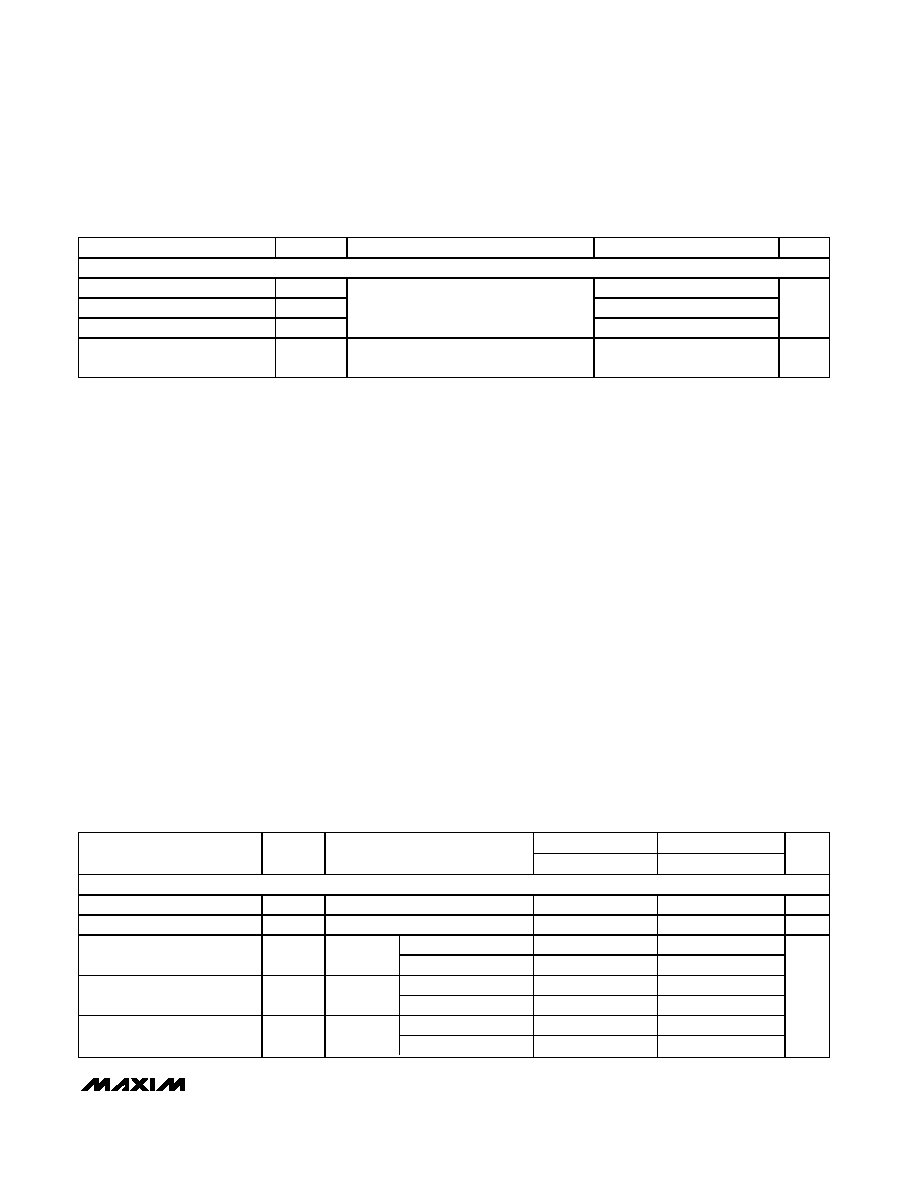
ABSOLUTE MAXIMUM RATINGS (DG201A)
Voltages Reference to V-
V+………………………………………………..……………..44V
GND……………………………………………..……….…….25V
Digital Inputs (Note 1), VS, VD ............................-2V to (V+ + 2V)
or 20mA, whichever occurs first
Current, Any Terminal Except S or D………..….…………...30mA
Continuous Current, S or D…………………………………...20mA
Peak Current, S or D
(pulsed at 1ms 10% duty cycle max)…………………….70mA
Operating Temperature Range
DG201AA .............…………........………..…...-55°C to +125°C
DG201AD/E .........………………….....…..….…-40°C to +85°C
DG201AC .............………........................…….…0°C to +70°C
Storage Temperature Range………………..…..-65°C to +150°C
Power Dissipation (Note 2)
16-Pin Plastic Dip (derate 10.5mW/°C above +70°C) ...842mW
16-Pin SO (derate 8.7mW/°C above +70°C) .................696mW
16-Pin TSSOP (derate 9.4mW/°C above +70°C) ...........755mW
16-Pin QFN (5 5)
(derate 19.2mW/°C above +70°C)...........................1538mW
16-Pin CERDIP (derate 10.0mW/°C above +70°C)......800mW
Stresses beyond those listed under “Absolute Maximum Ratings” may cause permanent damage to the device. These are stress ratings only, and functional
operation of the device at these or any other conditions beyond those indicated in the operational sections of the specifications is not implied. Exposure to
absolute maximum rating conditions for extended periods may affect device reliability.
DG201AA
DG201AC, D, E
PARAMETER
SYMBOL
CONDITIONS
MIN
TYP
MAX
MIN
TYP
MAX
UNITS
SWITCH
Analog Signal Range
VANALOG
-15
15
-15
15
V
Drain-Source ON Resistance
RDS (ON)
VD = ±10V, VIN = 0.8V, IS = 1mA
115
175
115
200
VS = 14V, VD = -14V
0.01
1.0
0.01
5.0
Source OFF-Leakage Current
IS (OFF)
VIN = 2.4V
VS = -14V, VD = 14V
-1.0
-0.02
-5.0
-0.02
VS = 14V, VD = -14V
0.01
1.0
0.01
5.0
Drain OFF-Leakage Current
ID (OFF)
VIN = 2.4V
VS = -14V, VD = 14V
-1.0
-0.02
-5.0
-0.02
VS = -14V
0.1
1.0
0.1
1.0
Drain ON-Leakage Current
(Note 4)
ID (ON)
VIN = 0.8V
VS = 14V
-1.0
nA
ELECTRICAL CHARACTERISTICS (DG201A)
(V+ = +15V, V- = -15V, GND = 0, TA = +25°C, unless otherwise noted.) (For more information on TYP values see Note 3.)
ELECTRICAL CHARACTERISTICS (DG211) (continued)
(V+ = +15V, V- = -15V, GND = 0, TA = +25°C, unless otherwise noted.) (For more information on TYP values see Note 2.)
PARAMETER
SYMBOL
CONDITIONS
MIN
TYP
MAX
UNITS
SUPPLY
Positive Supply Current
I
+
0.02
0.4
Negative Supply Current
I
-
0.01
0.4
Logic Supply Current
IL
VIN = 0 and 2.4V (all)
00
mA
Power-Supply Range
for Continous Operation
VOP
±4.5
±18
V
Note 1: Signals on S_, D_, or IN_ exceeding V+ or V- on Maxim’s DG201A will be clamped by internal diodes, and are also internally cur-
rent limited to 25mA.
Note 2: Device mounted with all leads soldered to PC board.
Note 2: Typical values are for DESIGN AID ONLY, not guaranteed nor subject to production testing.
Note 3: ID(ON) is leakage from driver into “ON” switch.
Note 4: OFF-Isolation = 20 log VS/VD, VS = input to OFF switch, VD = output.
相关PDF资料 |
PDF描述 |
|---|---|
| VI-B13-IY-F1 | CONVERTER MOD DC/DC 24V 50W |
| MAX321CPA+ | IC SWITCH DUAL SPST 8DIP |
| R5F100ACASP#V0 | MCU 16BIT 32KB FLASH 30SSOP |
| VI-213-IY-F4 | CONVERTER MOD DC/DC 24V 50W |
| MAX4053CSE+T | IC MULTIPLEXER TRPL 2X1 16SOIC |
相关代理商/技术参数 |
参数描述 |
|---|---|
| DG211SE | 制造商:未知厂家 制造商全称:未知厂家 功能描述:SPST Analog Switch |
| DG-211V | 制造商:KODENSHI 制造商全称:KODENSHI KOREA CORP. 功能描述:Photointerrupters(Transmissive) |
| DG212 | 制造商:INTERSIL 制造商全称:Intersil Corporation 功能描述:SPST 4-Channel Analog Switches |
| DG212 WAF | 制造商:Intersil Corporation 功能描述: |
| DG212B | 制造商:VISHAY 制造商全称:Vishay Siliconix 功能描述:Improved Quad CMOS Analog Switches |
发布紧急采购,3分钟左右您将得到回复。