- 您现在的位置:买卖IC网 > PDF目录11371 > DG2738DN-T1-E4 (Vishay Siliconix)IC SWTICH DUAL SPST 8-MINIQFN PDF资料下载
参数资料
| 型号: | DG2738DN-T1-E4 |
| 厂商: | Vishay Siliconix |
| 文件页数: | 4/10页 |
| 文件大小: | 0K |
| 描述: | IC SWTICH DUAL SPST 8-MINIQFN |
| 标准包装: | 1 |
| 功能: | 开关 |
| 电路: | 2 x SPST - NC/NO |
| 导通状态电阻: | 8 欧姆 |
| 电压电源: | 单电源 |
| 电压 - 电源,单路/双路(±): | 2.3 V ~ 4.3 V |
| 电流 - 电源: | 1µA |
| 工作温度: | -40°C ~ 85°C |
| 安装类型: | 表面贴装 |
| 封装/外壳: | 8-UFQFN |
| 供应商设备封装: | 8-迷你型QFN(1.4x1.4) |
| 包装: | 标准包装 |
| 其它名称: | DG2738DN-T1-E4DKR |
Document Number: 68801
S-82643-Rev. B, 03-Nov-08
www.vishay.com
3
Vishay Siliconix
DG2737, DG2738, DG2739
Notes:
a. Room = 25 °C, Full = as determined by the operating suffix.
b. The algebraic convention whereby the most negative value is a minimum and the most positive a maximum, is used in this data sheet.
c. Typical values are for design aid only, not guaranteed nor subject to production testing.
d. Guarantee by design, not subjected to production test.
e. VIN = input voltage to perform proper function.
Stresses beyond those listed under “Absolute Maximum Ratings” may cause permanent damage to the device. These are stress ratings only, and functional operation
of the device at these or any other conditions beyond those indicated in the operational sections of the specifications is not implied. Exposure to absolute maximum
rating conditions for extended periods may affect device reliability.
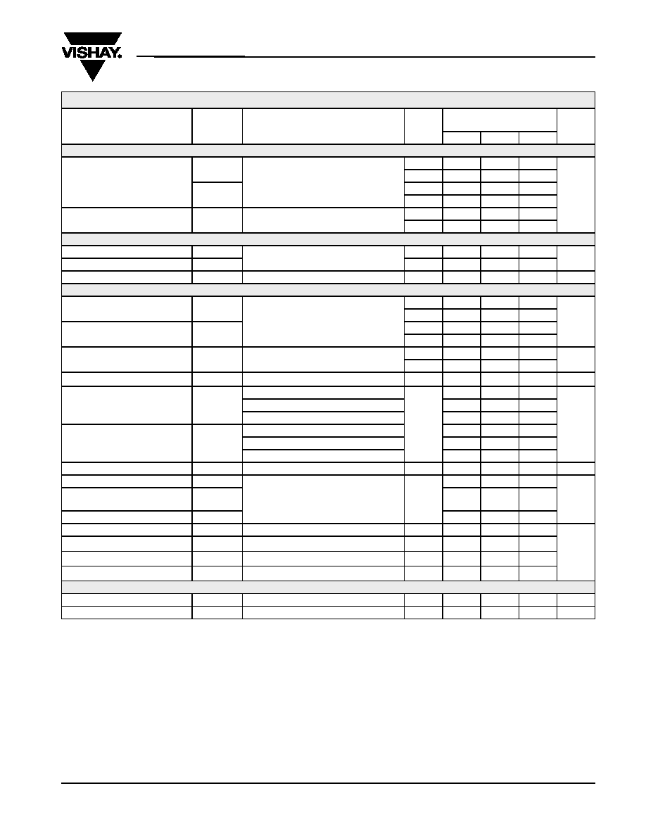
Parameter
Symbol
Test Conditions
Unless Otherwise Specified
V+ = 3 V, VIN = 0.4 V or 1.4 V
e
Temp.a
Limits
- 40 °C to 85 °C
Unit
Min.b
Typ.c
Max.b
Analog Switch
Switch Off Leakage
Current
IS(off)
V+ = 4.3 V, VS = 0.3 V/3.3 V,
VD = 3.3 V/0.3 V
Room
- 10
10
nA
Full
- 100
100
ID(off)
Room
- 10
10
Full
- 100
100
Channel-On Leakage Current
ID(on)
V+ = 4.3 V, VS = VD = 4 V/0.3 V
Room
- 10
10
Full
- 100
100
Digital Control
Input High Voltage
VINH
V+ = 2.3 V to 4.3 V
Full
1.3
V
Input Low Voltage
VINL
Full
0.5
Input Current
IINL or IINH
VIN = 0 or V+
Full
- 1
1
A
Dynamic Characteristics
Turn-On Timee
tON
V+ = 2.3 V to 3.6 V, VNO or VS = 1.5 V,
RL = 50 Ω, CL = 35 pF
Room
23
60
ns
Full
70
Turn-Off Timee
tOFF
Room
13
50
Full
60
Break-Before-Make Time
tBBM
V+ = 2.3 V to 4.3 V
Room
6
ns
Full
1
Charge Injectiond
Q
CL = 1 nF, RGEN = 0 Ω, VGEN = 0 V
Room
10.4
pC
Off-Isolationd
OIRR
RL = 50 Ω, CL = 5 pF, f = 1 MHz
Room
- 79
dB
RL = 50 Ω, CL = 5 pF, f = 10 MHz
- 59
RL = 50 Ω, CL = 5 pF, f = 240 MHz
- 28
Crosstalkd
XTALK
RL = 50 Ω, CL = 5 pF, f = 1 MHz
- 109
RL = 50 Ω, CL = 5 pF, f = 10 MHz
- 99
RL = 50 Ω, CL = 5 pF, f = 240 MHz
- 48
3 dB bandwidthd
RL = 50 Ω, CL = 5 pF
Room
720
MHz
Channel to Channel skewd
RL = 50 Ω, CL = 5 pF
Room
25
ps
Skew of Opposite Transitions
of the Same Outputd
20
Total Jitterd
200
Source Off Capacitanced
CS(off)
f = 1 MHz, VS = 0 V
Room
4.4
pF
Drain Off Capacitanced
CD(off)
f = 1 MHz, VD = 0 V
Room
3.8
Drain On Capacitanced
CD(on)
f = 1 MHz, VD = VS = 0 V
Room
10
Control Pin Capacitanced
CIN
f = 1 MHz
Room
8.3
Power Supply
Power Supply Range
V+
2.3
4.3
V
Power Supply Current
I+
VIN = 0 or V+
Full
1.0
A
SPECIFICATIONS V+ = 3 V
相关PDF资料 |
PDF描述 |
|---|---|
| PIC18F2525-E/SO | IC MCU FLASH 24KX16 28SOIC |
| GRM219R61C225KA88J | CAP CER 2.2UF 16V 10% X5R 0805 |
| PIC18F2220T-I/SO | IC MCU FLASH 2KX16 EEPROM 28SOIC |
| DEHR32E331KB2B | CAP CER 330PF 250V 10% RADIAL |
| PIC16C642-20I/SP | IC MCU OTP 4KX14 COMP 28DIP |
相关代理商/技术参数 |
参数描述 |
|---|---|
| DG2739 | 制造商:VISHAY 制造商全称:Vishay Siliconix 功能描述:6-Ω, Low Voltage, Dual SPST Analog Switch |
| DG2739DN-T1-E4 | 功能描述:模拟开关 IC Dual SPST Low Volt RoHS:否 制造商:Texas Instruments 开关数量:2 开关配置:SPDT 开启电阻(最大值):0.1 Ohms 切换电压(最大): 开启时间(最大值): 关闭时间(最大值): 工作电源电压:2.7 V to 4.5 V 最大工作温度:+ 85 C 安装风格:SMD/SMT 封装 / 箱体:DSBGA-16 |
| DG2741 | 制造商:VISHAY 制造商全称:Vishay Siliconix 功能描述:Low-Voltage, 0.8-ohm rON, Dual SPST Analog Switch |
| DG2741_11 | 制造商:VISHAY 制造商全称:Vishay Siliconix 功能描述:Low-Voltage, 0.8ohm RON, Dual SPST Analog Switch |
| DG2741DQ-T1 | 制造商:Vishay Semiconductors 功能描述: |
发布紧急采购,3分钟左右您将得到回复。