- 您现在的位置:买卖IC网 > PDF目录11130 > DG413CY+T (Maxim Integrated Products)IC SWITCH QUAD SPST 16SOIC PDF资料下载
参数资料
| 型号: | DG413CY+T |
| 厂商: | Maxim Integrated Products |
| 文件页数: | 5/12页 |
| 文件大小: | 0K |
| 描述: | IC SWITCH QUAD SPST 16SOIC |
| 产品培训模块: | Lead (SnPb) Finish for COTS Obsolescence Mitigation Program |
| 标准包装: | 2,500 |
| 功能: | 开关 |
| 电路: | 4 x SPST - NC/NO |
| 导通状态电阻: | 80 欧姆 |
| 电压电源: | 单/双电源 |
| 电压 - 电源,单路/双路(±): | 10 V ~ 30 V,±4.5 V ~ 20 V |
| 电流 - 电源: | 100pA |
| 工作温度: | 0°C ~ 70°C |
| 安装类型: | 表面贴装 |
| 封装/外壳: | 16-SOIC(0.154",3.90mm 宽) |
| 供应商设备封装: | 16-SOIC |
| 包装: | 带卷 (TR) |
DG411/DG412/DG413
Improved, Quad,
SPST Analog Switches
2
_______________________________________________________________________________________
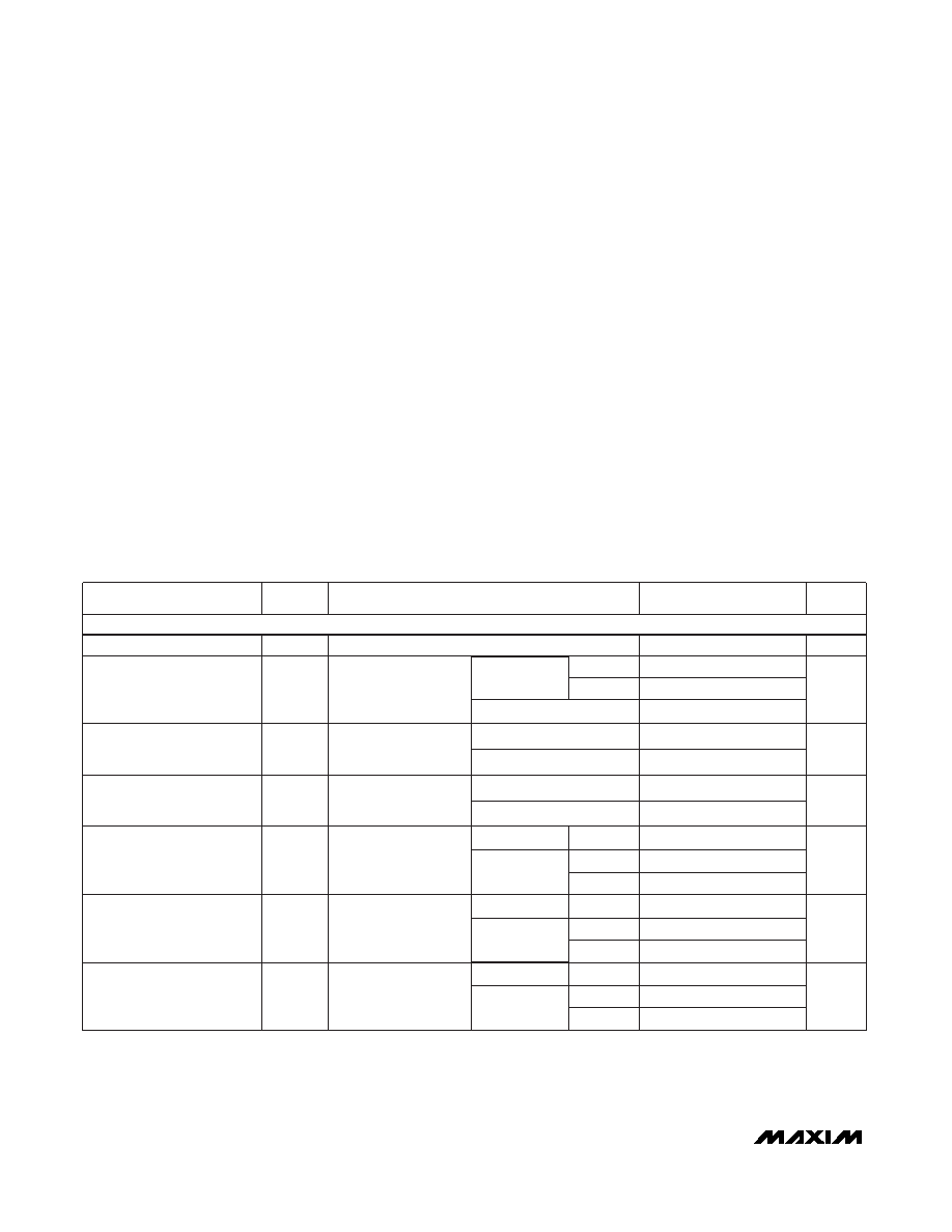
ABSOLUTE MAXIMUM RATINGS
ELECTRICAL CHARACTERISTICS—Dual Supplies
(V+ = 15V, V- = -15V, VL = 5V, VGND = 0V, VINH = 2.4V, VINL = 0.8V, TA = TMIN to TMAX, unless otherwise noted.)
Stresses beyond those listed under “Absolute Maximum Ratings” may cause permanent damage to the device. These are stress ratings only, and functional
operation of the device at these or any other conditions beyond those indicated in the operational sections of the specifications is not implied. Exposure to
absolute maximum rating conditions for extended periods may affect device reliability.
Note 1: Signals on S, D, or IN exceeding V+ or V- are clamped by internal diodes. Limit forward current to maximum
current rating.
(All Voltages Referenced to V-.)
V+.........................................................................................44V
GND .....................................................................................25V
VL .....................................................(GND -0.3V) to (V+ +0.3V)
Digital Inputs, VS, VD (Note 1)........(V- -2V) to (V+ +2V) or 30mA
(whichever occurs first)
Continuous Current (any terminal) ......................................30mA
Peak Current
(pulsed at 1ms, 10% duty cycle max) ............................100mA
Continuous Power Dissipation (TA = +70°C)
16-Pin Plastic DIP (derate 10.53mW/°C above +70°C) .842mW
16-Pin Narrow SO (derate 8.70mW/°C above +70°C) ...696mW
16-Pin CERDIP (derate 10.00mW/°C above +70°C)......800mW
16-Pin TSSOP (derate 6.7mW/°C above +70°C) ...........457mW
16-Pin QFN (derate 19.2mW/°C above +70°C) ...........1538mW
Operating Temperature Ranges
DG41_C_ ..............................................................0°C to +70°C
DG41_D_ ...........................................................-40°C to +85°C
DG41_AK_ .......................................................-55°C to +125°C
Storage Temperature Range .............................-65°C to +150°C
Lead Temperature (soldering, 10s) .................................+300°C
17
30
A
C, D
-40
40
-10
10
-10
10
-0.25
-0.10
0.25
6
5
A
TA = TMIN to TMAX
C, D
TA = TMIN to TMAX
TA = +25°C
TA = TMIN to
TMAX
TA = +25°C
TA = TMIN to
TMAX
TA = +25°C
TA = TMIN to
TMAX
TA = +25°C
V+ = 16.5V,
V- = -16.5V,
VD = ±15.5V,
VS = ±15.5V
V+ = 16.5V,
V- = -16.5V,
VD = ±15.5V,
VS = ±15.5V
(Note 3)
V+ = 16.5V,
V- = -16.5V,
VD = ±15.5V,
VS = ±15.5V
V+ = 15V, V- = -15V,
VD = ±10V,
IS = -10mA
V+ = 13.5V,
V- = -13.5V,
VD = ±8.5V,
IS = -10mA
V+ = 15V, V- = -15V,
VD = ±5V, 0V,
IS = -10mA
CONDITIONS
nA
-20
20
ID(ON)
+
IS(ON)
Drain On-Leakage Current
(Note 7)
-0.4
-0.1
0.4
ID(OFF)
nA
-5
5
Drain Off-Leakage Current
(Note 7)
-5
5
nA
IS(OFF)
Source Off-Leakage Current
(Note 7)
-0.25
-0.10
0.25
Ω
4
RFLAT(ON)
On-Resistance Flatness
(Note 4)
V
-15
15
VANALOG
Analog Signal Range
ΔRDS(ON)
On-Resistance
Match Between Channels
(Note 4)
Ω
3
17
45
Ω
45
RDS(ON)
Drain-Source
On-Resistance
UNITS
MIN
TYP
MAX
(Note 2)
SYMBOL
PARAMETER
C, D, A
SWITCH
相关PDF资料 |
PDF描述 |
|---|---|
| DG412CY+T | IC SWITCH QUAD SPST 16SOIC |
| MAX4588CAI+T | IC RF/VIDEO MUX DUAL 4CH 28-SSOP |
| DG412EUE+G002 | IC SWITCH QUAD SPST 16TSSOP |
| DG509ADY+T | IC MULTIPLEXER DUAL 4X1 16SOIC |
| DG508ADY+T | IC MULTIPLEXER 8X1 16SOIC |
相关代理商/技术参数 |
参数描述 |
|---|---|
| DG413CY-TG068 | 制造商:Maxim Integrated Products 功能描述:16 PINS N.SO PKG - Bulk |
| DG413DJ | 功能描述:模拟开关 IC Quad SPST Switch RoHS:否 制造商:Texas Instruments 开关数量:2 开关配置:SPDT 开启电阻(最大值):0.1 Ohms 切换电压(最大): 开启时间(最大值): 关闭时间(最大值): 工作电源电压:2.7 V to 4.5 V 最大工作温度:+ 85 C 安装风格:SMD/SMT 封装 / 箱体:DSBGA-16 |
| DG413DJ | 制造商:Vishay Siliconix 功能描述:IC SWITCH QUAD SPST DIP16 413 |
| DG413DJ+ | 功能描述:模拟开关 IC Quad SPST Open/Closed RoHS:否 制造商:Texas Instruments 开关数量:2 开关配置:SPDT 开启电阻(最大值):0.1 Ohms 切换电压(最大): 开启时间(最大值): 关闭时间(最大值): 工作电源电压:2.7 V to 4.5 V 最大工作温度:+ 85 C 安装风格:SMD/SMT 封装 / 箱体:DSBGA-16 |
| DG413DJ-E3 | 功能描述:模拟开关 IC Quad SPST Switch RoHS:否 制造商:Texas Instruments 开关数量:2 开关配置:SPDT 开启电阻(最大值):0.1 Ohms 切换电压(最大): 开启时间(最大值): 关闭时间(最大值): 工作电源电压:2.7 V to 4.5 V 最大工作温度:+ 85 C 安装风格:SMD/SMT 封装 / 箱体:DSBGA-16 |
发布紧急采购,3分钟左右您将得到回复。