- 您现在的位置:买卖IC网 > PDF目录11149 > DG417CY+T (Maxim Integrated Products)IC SWITCH SPST 8SOIC PDF资料下载
参数资料
| 型号: | DG417CY+T |
| 厂商: | Maxim Integrated Products |
| 文件页数: | 9/12页 |
| 文件大小: | 0K |
| 描述: | IC SWITCH SPST 8SOIC |
| 产品培训模块: | Lead (SnPb) Finish for COTS Obsolescence Mitigation Program |
| 标准包装: | 2,500 |
| 功能: | 开关 |
| 电路: | 1 x SPST- NC |
| 导通状态电阻: | 100 欧姆 |
| 电压电源: | 单/双电源 |
| 电压 - 电源,单路/双路(±): | 10 V ~ 30 V,±4.5 V ~ 20 V |
| 电流 - 电源: | 100pA |
| 工作温度: | 0°C ~ 70°C |
| 安装类型: | 表面贴装 |
| 封装/外壳: | 8-SOIC(0.154",3.90mm 宽) |
| 供应商设备封装: | 8-SOIC |
| 包装: | 带卷 (TR) |
DG417/DG418/DG419
__________Applications Information
Operation with Supply Voltages
Other than ±15V
Using supply voltages other than ±15V reduces the
analog signal range. The DG417/DG418/DG419 switch-
es operate with ±4.5V to ±20V bipolar supplies or with
a +10V to +30V single supply; connect V- to 0V when
operating with a single supply. Also, all device types
can operate with unbalanced supplies, such as +24V
and -5V. VL must be connected to +5V to be TTL com-
patible, or to V+ for CMOS-logic level inputs. The
Typical Operating Characteristics graphs show typical
on-resistance with ±20V, ±15V, ±10V, and ±5V sup-
plies. (Switching times increase by a factor of two or
more for operation at ±5V.)
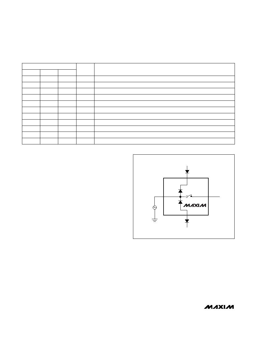
Overvoltage Protection
Proper power-supply sequencing is recommended for
all CMOS devices. Do not exceed the absolute maxi-
mum ratings because stresses beyond the listed rat-
ings may cause permanent damage to the devices.
Always sequence V+ on first, followed by VL, V-, and
logic inputs. If power-supply sequencing is not possi-
ble, add two small, external signal diodes in series with
the supply pins for overvoltage protection (Figure 1).
Adding diodes reduces the analog signal range to 1V
below V+ and 1V above V-, without affecting low switch
resistance and low leakage characteristics. Device
operation is unchanged, and the difference between
V+ and V- should not exceed +44V.
Improved, SPST/SPDT Analog Switches
6
_______________________________________________________________________________________
______________________________________________________________Pin Description
FUNCTION
DG417
DG418
1
—
Analog-Switch Source Terminal (normally closed)
PIN
—
1
Analog-Switch Source Terminal (normally open)
2
No Internal Connection
6
Logic-Level Input
5
Logic-Level Positive Supply Input
4
Analog-Signal Positive Supply Input
3
Logic Ground
7
Analog-Signal Negative Supply Input
V+
D
V-
S
Vg
DG41_
Figure 1. Overvoltage Protection Using External Blocking Diodes
NAME
DG419
—
S
—
S
—
N.C.
6
IN
5
VL
4
V+
3
GND
7
V-
8
Analog-Switch Drain Terminal
1
D
—
Analog-Switch Source Terminal 1 (normally closed)
2
S1
—
Analog-Switch Source Terminal 2 (normally open)
8
S2
相关PDF资料 |
PDF描述 |
|---|---|
| MAX4850ETE+T | IC SWITCH DUAL SPDT 16TQFN |
| MAX4525CUB+T | IC MULTIPLEXER 2X2 10UMAX |
| VI-BNF-IW-F2 | CONVERTER MOD DC/DC 72V 100W |
| VE-21N-IY-F1 | CONVERTER MOD DC/DC 18.5V 50W |
| MAX4524CUB+T | IC MULTIPLEXER 4X1 10UMAX |
相关代理商/技术参数 |
参数描述 |
|---|---|
| DG417DJ | 功能描述:模拟开关 IC SPST Analog Switch RoHS:否 制造商:Texas Instruments 开关数量:2 开关配置:SPDT 开启电阻(最大值):0.1 Ohms 切换电压(最大): 开启时间(最大值): 关闭时间(最大值): 工作电源电压:2.7 V to 4.5 V 最大工作温度:+ 85 C 安装风格:SMD/SMT 封装 / 箱体:DSBGA-16 |
| DG417DJ | 制造商:Vishay Siliconix 功能描述:IC SWITCH SPDT DIP8 417 |
| DG417DJ-E3 | 功能描述:模拟开关 IC SPST Analog Switch RoHS:否 制造商:Texas Instruments 开关数量:2 开关配置:SPDT 开启电阻(最大值):0.1 Ohms 切换电压(最大): 开启时间(最大值): 关闭时间(最大值): 工作电源电压:2.7 V to 4.5 V 最大工作温度:+ 85 C 安装风格:SMD/SMT 封装 / 箱体:DSBGA-16 |
| DG417DK | 功能描述:模拟开关 IC RoHS:否 制造商:Texas Instruments 开关数量:2 开关配置:SPDT 开启电阻(最大值):0.1 Ohms 切换电压(最大): 开启时间(最大值): 关闭时间(最大值): 工作电源电压:2.7 V to 4.5 V 最大工作温度:+ 85 C 安装风格:SMD/SMT 封装 / 箱体:DSBGA-16 |
| DG417DY | 功能描述:模拟开关 IC SPST Analog Switch RoHS:否 制造商:Texas Instruments 开关数量:2 开关配置:SPDT 开启电阻(最大值):0.1 Ohms 切换电压(最大): 开启时间(最大值): 关闭时间(最大值): 工作电源电压:2.7 V to 4.5 V 最大工作温度:+ 85 C 安装风格:SMD/SMT 封装 / 箱体:DSBGA-16 |
发布紧急采购,3分钟左右您将得到回复。