- 您现在的位置:买卖IC网 > PDF目录11506 > DG428DN-E3 (Vishay Siliconix)IC MUX ANLG 8CH W/LATCH 20PLCC PDF资料下载
参数资料
| 型号: | DG428DN-E3 |
| 厂商: | Vishay Siliconix |
| 文件页数: | 3/14页 |
| 文件大小: | 0K |
| 描述: | IC MUX ANLG 8CH W/LATCH 20PLCC |
| 标准包装: | 500 |
| 功能: | 多路复用器 |
| 电路: | 1 x 8:1 |
| 导通状态电阻: | 150 欧姆 |
| 电压电源: | 单/双电源 |
| 电压 - 电源,单路/双路(±): | 12V,±15V |
| 电流 - 电源: | 20µA |
| 工作温度: | -40°C ~ 85°C |
| 安装类型: | 表面贴装 |
| 封装/外壳: | 20-LCC(J 形引线) |
| 供应商设备封装: | 20-PLCC(9x9) |
| 包装: | 管件 |
Document Number: 70063
S11-1350–Rev. K, 04-Jul-11
www.vishay.com
11
Vishay Siliconix
DG428, DG429
This document is subject to change without notice.
THE PRODUCTS DESCRIBED HEREIN AND THIS DOCUMENT ARE SUBJECT TO SPECIFIC DISCLAIMERS, SET FORTH AT www.vishay.com/doc?91000
DETAILED DESCRIPTION
The internal structure of the DG428, DG429 includes a 5 V
logic interface with input protection circuitry followed by a
latch, level shifter, decoder and finally the switch constructed
with parallel n- and p-channel MOSFETs (see Figure 1).
The input protection on the logic lines A0, A1, A2, EN and
control lines WR, RS shown in Figure 1 minimizes
susceptibility to ESD that may be encountered during
handling and operational transients.
The logic interface is a CMOS logic input with its supply
voltage from an internal + 5 V reference voltage. The output
of the input inverter feeds the data input of a D type latch.
The level sensitive D latch continuously places the DX input
signal on the QX output when the WR input is low, resulting
in transparent latch operation. As soon as WR returns high
the latch holds the data last present on the Dn input, subject
to the "Minimum Input Timing Requirements" table.
Following the latches the Qn signals are level shifted and
decoded to provide proper drive levels for the CMOS
switches. This level shifting ensures full on/off switch
operation for any analog signal level between the V+ and
V- supply rails.
The EN pin is used to enable the address latches during the
WR pulse. It can be hard wired to the logic supply or to V+ if
one of the channels will always be used (except during a
reset) or it can be tied to address decoding circuitry for
memory mapped operation. The RS pin is used as a master
reset. All latches are cleared regardless of the state of any
other latch or control line. The WR pin is used to transfer the
state of the address control lines to their latches, except
during a reset or when EN is low (see Truth Tables).
APPLICATIONS HINTS
Bus Interfacing
The DG428, DG429 minimize the amount of interface
hardware between a microprocessor system bus and the
analog system being controlled or measured. The internal
TTL compatible latches give these multiplexers write-only
memory, that is, they can be programmed to stay in a
particular switch state (e.g., switch 1 on) until the
microprocessor determines it is necessary to turn different
switches on or turn all switches off (see Figure 10).
The input latches become transparent when WR is held low;
therefore, these multiplexers operate by direct command of
the coded switch state on A2, A1, A0. In this mode the DG428
is identical to the popular DG408. The same is true of the
DG429 versus the popular DG409.
During system power-up, RS would be low, maintaining all
eight switches in the off state. After RS returned high the
DG428 maintains all switches in the off state.
When the system program performs a write operation to the
address assigned to the DG428, the address decoder
provides a CS active low signal which is gated with the
WRITE (WR) control signal. At this time the data on the
DATA BUS (that will determine which switch to close) is
stabilizing. When the WR signal returns to the high state,
(positive edge) the input latches of the DG428 save the data
from the DATA BUS. The coded information in the A0, A1, A2
and EN latches is decoded and the appropriate switch is
turned on.
The EN latch allows all switches to be turned off under
program control. This becomes useful when two or more
DG428s
are
cascaded
to
build
16-line
and
larger
multiplexers.
Vishay Siliconix maintains worldwide manufacturing capability. Products may be manufactured at one of several qualified locations. Reliability data for Silicon Tech-
nology and Package Reliability represent a composite of all qualified locations. For related documents such as package/tape drawings, part marking, and reliability
data, see www.vishay.com/ppg?70063.
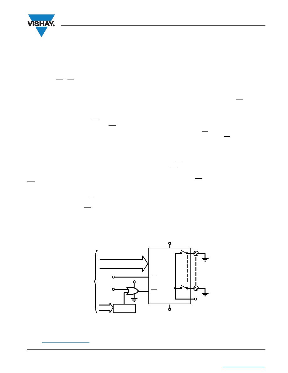
Figure 10. Bus Interface
Data Bus
RESET
Address
Decoder
Address
Bus
+ 5 V
V+
V-
D
+ 15 V
- 15 V
DG428
Processor
System
Bus
15 V
Analog
Inputs
Analog
Output
WR
RS
S1
S8
A0, A1, A2, EN
WRITE
相关PDF资料 |
PDF描述 |
|---|---|
| PIC16LC717/SS | IC MCU OTP 2KX14 A/D PWM 20SSOP |
| DG333ALDW-E3 | IC SWITCH QUAD SPDT 20SOIC |
| VI-B3X-CU-F4 | CONVERTER MOD DC/DC 5.2V 200W |
| DG333ADW-E3 | IC SWITCH QUAD SPDT 20SOIC |
| PIC16C711T-04/SO | IC MCU OTP 1KX14 A/D 18SOIC |
相关代理商/技术参数 |
参数描述 |
|---|---|
| DG428DN-T1 | 制造商:Vishay Intertechnologies 功能描述: |
| DG429 | 制造商:INTERSIL 制造商全称:Intersil Corporation 功能描述:2 CHANNEL DRIVERS WITH SPST AND DPST FET SWITCHES |
| DG429A | 制造商:INTERSIL 制造商全称:Intersil Corporation 功能描述:2 CHANNEL DRIVERS WITH SPST AND DPST FET SWITCHES |
| DG429AK | 制造商:未知厂家 制造商全称:未知厂家 功能描述:4-Channel Analog Multiplexer |
| DG429AK/883 | 制造商:未知厂家 制造商全称:未知厂家 功能描述:4-Channel Analog Multiplexer |
发布紧急采购,3分钟左右您将得到回复。