- 您现在的位置:买卖IC网 > PDF目录11056 > DG442CJ (Maxim Integrated Products)IC SWITCH QUAD SPST 16DIP PDF资料下载
参数资料
| 型号: | DG442CJ |
| 厂商: | Maxim Integrated Products |
| 文件页数: | 4/9页 |
| 文件大小: | 0K |
| 描述: | IC SWITCH QUAD SPST 16DIP |
| 产品培训模块: | Lead (SnPb) Finish for COTS Obsolescence Mitigation Program |
| 标准包装: | 25 |
| 功能: | 开关 |
| 电路: | 4 x SPST - NO |
| 导通状态电阻: | 160 欧姆 |
| 电压电源: | 单/双电源 |
| 电压 - 电源,单路/双路(±): | 10 V ~ 30 V,±4.5 V ~ 20 V |
| 工作温度: | 0°C ~ 70°C |
| 安装类型: | 通孔 |
| 封装/外壳: | 16-DIP(0.300",7.62mm) |
| 供应商设备封装: | 16-PDIP |
| 包装: | 管件 |
DG441/DG442
Improved, Quad, SPST Analog Switches
4
_______________________________________________________________________________________
ELECTRICAL CHARACTERISTICS—Single Supply
(V+ = 12V, V- = 0V, VGND = 0V, VINH = 2.4V, VINL = 0.8V, TA = TMIN to TMAX, unless otherwise noted.)
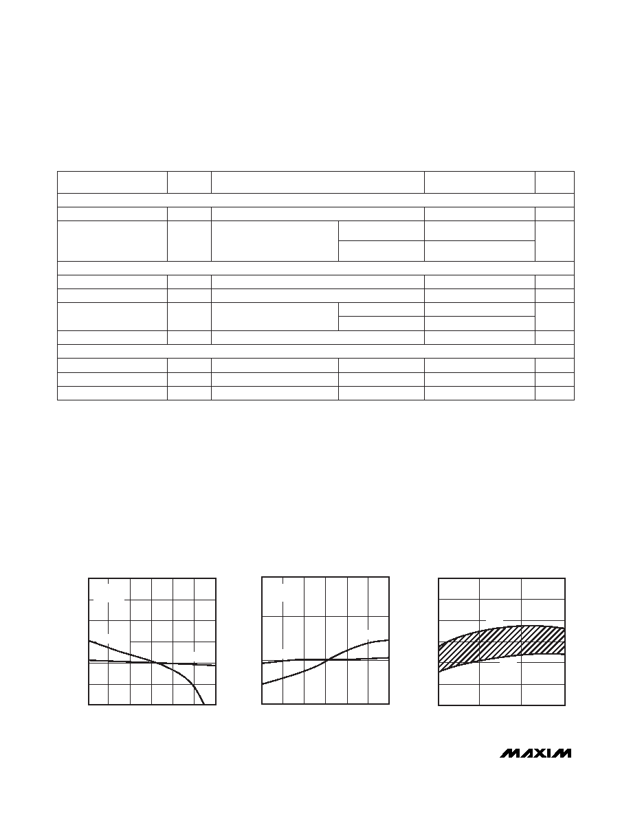
__________________________________________Typical Operating Characteristics
(TA = +25°C, unless otherwise noted.)
-15
0
15
-10
-5
510
ON-LEAKAGE CURRENTS
ON-LEAKAGE
(nA)
-2
-1
0
1
2
3
4
VS, VD (V)
TA = +125
°C
TA = +85
°C
V+ = 15V
V- = -15V
-15
0
15
-10
-5
510
OFF-LEAKAGE CURRENTS
OFF-LEAKAGE
(nA)
-1
0
2
1
VS, VD (V)
TA = +85
°C
TA = +125
°C
V+ = 15V
V- = -15V
SWITCHING THRESHOLD vs.
BIPOLAR SUPPLY VOLTAGE
V
IN
(V)
0
0.5
1.5
2.0
2.5
3.0
3.5
±5
±10
±15
±20
BIPOLAR SUPPLY VOLTAGE (V)
MAX
MIN
Note 2: Typical values are for design aid only, are not guaranteed, and are not subject to production testing. The algebraic con-
vention, where the most negative value is a minimum and the most positive value a maximum, is used in this data sheet.
Note 3: Guaranteed by design.
Note 4: On-resistance match between channels and flatness is guaranteed only with bipolar-supply operation. Flatness is defined
as the difference between the maximum and the minimum value of on-resistance as measured at the extremes of the speci-
fied analog range.
Note 5: Leakage parameters IS(OFF), ID(OFF), and ID(ON) are 100% tested at the maximum rated hot temperature and guaranteed
by correlation at +25°C.
Note 6: Off-Isolation Rejection Ratio = 20log (VD/VS), VD = output, VS = input to off switch.
Note 7: Between any two switches.
TA = +25°C
TA = TMIN to TMAX
A
(Note 3)
TA = +25°C
A
15
100
All channels on or off, VIN = 0V or 5V
I+
TA = TMIN to TMAX
Positive Supply Current
TA = +25°C
CL = 1nF, VGEN = 0V
ns
V+ = 10.8V, VD = 3V, 8V,
IS = 1.0mA
60
200
Q
Charge Injection (Note 3)
pC
510
CONDITIONS
-5
5
VS = 8V, Figure 2
tOFF
Turn-Off Time
TA = +25°C
All channels on or off,
VIN = 0V or 5V
V
-100
-15
All channels on or off, VIN = 0V or 5V
IGND
Ground Current
TA = +25°C
V
012
VANALOG
Analog Signal Range
10
30
I-
Negative Supply Current
A
-1
-0.0001
1
V+
Ω
100
160
rDS(ON)
Drain-Source
On-Resistance
200
Power-Supply Range
VS = 8V, Figure 2
tON
Turn-On Time
ns
UNITS
MIN
TYP
MAX
(Note 2)
SYMBOL
PARAMETER
300
400
SWITCH
SUPPLY
DYNAMIC
相关PDF资料 |
PDF描述 |
|---|---|
| MAX306EQI | IC MULTIPLEXER 16X1 28PLCC |
| DG419CY | IC SWITCH SPDT 8SOIC |
| MAX4528CPA | IC SWITCH DUAL SPDT 8DIP |
| MAX313CSE | IC SWITCH QUAD SPST 16SOIC |
| MAX379CPE | IC MULTIPLEXER DUAL 4X1 16DIP |
相关代理商/技术参数 |
参数描述 |
|---|---|
| DG442CJ+ | 功能描述:模拟开关 IC Quad SPST CMOS Normally Open RoHS:否 制造商:Texas Instruments 开关数量:2 开关配置:SPDT 开启电阻(最大值):0.1 Ohms 切换电压(最大): 开启时间(最大值): 关闭时间(最大值): 工作电源电压:2.7 V to 4.5 V 最大工作温度:+ 85 C 安装风格:SMD/SMT 封装 / 箱体:DSBGA-16 |
| DG442CY | 功能描述:模拟开关 IC RoHS:否 制造商:Texas Instruments 开关数量:2 开关配置:SPDT 开启电阻(最大值):0.1 Ohms 切换电压(最大): 开启时间(最大值): 关闭时间(最大值): 工作电源电压:2.7 V to 4.5 V 最大工作温度:+ 85 C 安装风格:SMD/SMT 封装 / 箱体:DSBGA-16 |
| DG442CY+ | 功能描述:模拟开关 IC Quad SPST CMOS Normally Open RoHS:否 制造商:Texas Instruments 开关数量:2 开关配置:SPDT 开启电阻(最大值):0.1 Ohms 切换电压(最大): 开启时间(最大值): 关闭时间(最大值): 工作电源电压:2.7 V to 4.5 V 最大工作温度:+ 85 C 安装风格:SMD/SMT 封装 / 箱体:DSBGA-16 |
| DG442CY+T | 功能描述:模拟开关 IC Quad SPST CMOS Normally Open RoHS:否 制造商:Texas Instruments 开关数量:2 开关配置:SPDT 开启电阻(最大值):0.1 Ohms 切换电压(最大): 开启时间(最大值): 关闭时间(最大值): 工作电源电压:2.7 V to 4.5 V 最大工作温度:+ 85 C 安装风格:SMD/SMT 封装 / 箱体:DSBGA-16 |
| DG442CY-T | 功能描述:模拟开关 IC RoHS:否 制造商:Texas Instruments 开关数量:2 开关配置:SPDT 开启电阻(最大值):0.1 Ohms 切换电压(最大): 开启时间(最大值): 关闭时间(最大值): 工作电源电压:2.7 V to 4.5 V 最大工作温度:+ 85 C 安装风格:SMD/SMT 封装 / 箱体:DSBGA-16 |
发布紧急采购,3分钟左右您将得到回复。