参数资料
| 型号: | DG445DY |
| 厂商: | Maxim Integrated Products |
| 文件页数: | 7/10页 |
| 文件大小: | 0K |
| 描述: | IC SWITCH QUAD SPST 16SOIC |
| 产品培训模块: | Lead (SnPb) Finish for COTS Obsolescence Mitigation Program |
| 标准包装: | 50 |
| 功能: | 开关 |
| 电路: | 4 x SPST - NO |
| 导通状态电阻: | 160 欧姆 |
| 电压电源: | 单/双电源 |
| 电压 - 电源,单路/双路(±): | 10 V ~ 30 V,±4.5 V ~ 20 V |
| 工作温度: | -40°C ~ 85°C |
| 安装类型: | 表面贴装 |
| 封装/外壳: | 16-SOIC(0.154",3.90mm 宽) |
| 供应商设备封装: | 16-SOIC |
| 包装: | 管件 |
DG444/DG445
Improved, Quad, SPST Analog Switches
6
_______________________________________________________________________________________
tOFF
0.8 x VOUT
VOUT
0.8 x VOUT
tf < 20ns
tr < 20ns
50%
0V
+3V
SWITCH
OUTPUT
LOGIC INPUT WAVEFORM IS INVERTED FOR SWITCHES
THAT HAVE THE OPPOSITE LOGIC SENSE.
tON
SWITCH
INPUT
LOGIC
INPUT
+3V
IN
+5V
V-
-15V
(
)
RL
CL
VOUT
S
CL INCLUDES FIXTURE AND STRAY CAPACITANCE.
GND
REPEAT TEST FOR CHANNELS 2, 3, AND 4.
VOUT = VD
RL
RL + rDS(ON)
LOGIC
INPUT
VL
+15V
V+
D
DG444
DG445
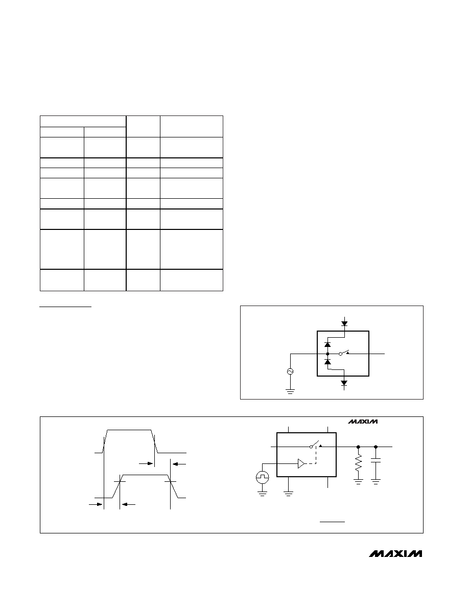
Figure 2. Switching Time
Applications Information
General Operation
Switches are open when power is off.
IN, D, and S should not exceed V+ or V-, even with
the power off.
Switch leakage is from each analog switch terminal
to V+ or V-, not to other switch terminals.
Operation with Supply Voltages
Other than ±15V
Using supply voltages other than ±15V will reduce the
analog signal range. The DG444/DG445 switches oper-
ate with ±4.5V to ±20V bipolar supplies or with a +10V
to +30V single supply; connect V- to 0V when operating
with a single supply. Also, all device types can operate
with unbalanced supplies such as +24V and -5V. VL
must be connected to +5V to be TTL compatible, or to
V+ for CMOS-logic level inputs. The Typical Operating
Characteristics graphs show typical on-resistance with
±20V, ±15V, ±10V, and ±5V supplies. (Switching times
increase by a factor of two or more for operation at ±5V.)
Overvoltage Protection
Proper power-supply sequencing is recommended
for all CMOS devices. Do not exceed the absolute
maximum ratings because stresses beyond the list-
ed ratings may cause permanent damage to the
devices. Always sequence V+ on first, followed by
VL , V-, and logic inputs. If power-supply sequenc-
ing is not possible, add two small, external signal
diodes in series with supply pins for overvoltage
protection (Figure 1). Adding diodes reduces the
analog signal range to 1V below V+ and 1V above
V-, but low switch resistance and low leakage char-
acteristics are unaffected. Device operation is
unchanged, and the difference between V+ and V-
should not exceed +44V.
V+
D
V-
S
Vg
Figure 1. Overvoltage Protection Using External Blocking Diodes
_____________________Pin Description
PIN
DIP/SO
THIN QFN
NAME
FUNCTION
1, 16, 9, 8
15, 14, 7, 6
IN1–IN4
Logic Control
Inputs
2, 15, 10, 7
16, 13, 8, 5
D1–D4
Drain Outputs
3, 14, 11, 6
1, 12, 9 4
S1–S4
Source Outputs
42
V-
Negative-Supply
Voltage Input
53
GND
Ground
12
10
VL
Logic-Supply
Voltage Input
13
11
V+
Positive-Supply-
Voltage
Input—Connected
to Substrate
—EP
PAD
Exposed Pad
Connect Pad to V+
相关PDF资料 |
PDF描述 |
|---|---|
| DG4599DL-T1-E3-HF | IC SWITCH SINGLE SPDT SC70-6 |
| DG459DJ-E3 | IC MUX ANALOG SINGLE 8CH 16DIP |
| DG506AEWI+ | IC MULTIPLEXER 16X1 28SOIC |
| DG507BEN-T1-GE3 | IC MUX ANA DUAL 16/8CH 28PLCC |
| DG508ACJZ | IC MULTIPLEXER 8X1 16DIP |
相关代理商/技术参数 |
参数描述 |
|---|---|
| DG445DY+ | 功能描述:模拟开关 IC Quad SPST CMOS Normally Open RoHS:否 制造商:Texas Instruments 开关数量:2 开关配置:SPDT 开启电阻(最大值):0.1 Ohms 切换电压(最大): 开启时间(最大值): 关闭时间(最大值): 工作电源电压:2.7 V to 4.5 V 最大工作温度:+ 85 C 安装风格:SMD/SMT 封装 / 箱体:DSBGA-16 |
| DG445DY+T | 功能描述:模拟开关 IC Quad SPST CMOS Normally Open RoHS:否 制造商:Texas Instruments 开关数量:2 开关配置:SPDT 开启电阻(最大值):0.1 Ohms 切换电压(最大): 开启时间(最大值): 关闭时间(最大值): 工作电源电压:2.7 V to 4.5 V 最大工作温度:+ 85 C 安装风格:SMD/SMT 封装 / 箱体:DSBGA-16 |
| DG445DY-E3 | 功能描述:模拟开关 IC SPST Analog Switch RoHS:否 制造商:Texas Instruments 开关数量:2 开关配置:SPDT 开启电阻(最大值):0.1 Ohms 切换电压(最大): 开启时间(最大值): 关闭时间(最大值): 工作电源电压:2.7 V to 4.5 V 最大工作温度:+ 85 C 安装风格:SMD/SMT 封装 / 箱体:DSBGA-16 |
| DG445DYR4546 | 制造商:Rochester Electronics LLC 功能描述:- Bulk |
| DG445DY-T | 功能描述:模拟开关 IC RoHS:否 制造商:Texas Instruments 开关数量:2 开关配置:SPDT 开启电阻(最大值):0.1 Ohms 切换电压(最大): 开启时间(最大值): 关闭时间(最大值): 工作电源电压:2.7 V to 4.5 V 最大工作温度:+ 85 C 安装风格:SMD/SMT 封装 / 箱体:DSBGA-16 |
发布紧急采购,3分钟左右您将得到回复。