- 您现在的位置:买卖IC网 > PDF目录11122 > DG528CCWN+ (Maxim Integrated Products)IC MULTIPLEXER 8X1 18SOIC PDF资料下载
参数资料
| 型号: | DG528CCWN+ |
| 厂商: | Maxim Integrated Products |
| 文件页数: | 10/12页 |
| 文件大小: | 0K |
| 描述: | IC MULTIPLEXER 8X1 18SOIC |
| 产品培训模块: | Lead (SnPb) Finish for COTS Obsolescence Mitigation Program |
| 标准包装: | 40 |
| 功能: | 多路复用器 |
| 电路: | 1 x 8:1 |
| 导通状态电阻: | 400 欧姆 |
| 电压电源: | 单/双电源 |
| 电压 - 电源,单路/双路(±): | 5 V ~ 30 V,±4.5 V ~ 20 V |
| 工作温度: | 0°C ~ 70°C |
| 安装类型: | 表面贴装 |
| 封装/外壳: | 18-SOIC(0.295",7.50mm 宽) |
| 供应商设备封装: | 18-SOIC W |
| 包装: | 管件 |
_______________Detailed Description
The internal structures of the DG528/DG529 include
translators for the A2/A1/A0/EN/WR/RS digital inputs,
latches, and a decode section for channel selection
(Truth Tables). The gate structures consist of parallel
combinations of N and P MOSFETs.
WRITE (WR) and RESET (RS) strobes are provided for
interfacing with P-bus lines (Figure 9), alleviating the
need for the P to provide constant address inputs to
the mux to hold a particular channel.
When the WR strobe is in the low state (less than 0.8V)
and the RS strobe is in the high state (greater than
2.4V), the muxes are in the transparent mode—they act
similarly to nonlatching devices, such as the DG508A/
DG509A or the HI508/HI509.
When the WR goes high, the previous BCD address
input is latched and held in that state indefinitely. To
pull the mux out of this state, either WR must be taken
low to the transition state, or RS must be taken low to
turn off all channels.
RS turns off all channels when it is low, which resets
channel selection to the channel 1 mode.
The DG528/DG529 work with both single and dual sup-
plies and function over the +5V to +30V single-supply
range. For example, with a single +15V power supply,
analog signals in the 0V to +15V range can be
switched normally. If negative signals around 0V are
expected, a negative supply is needed. However, only
-5V is needed to normally switch signals in the -5V to
+15V range (-5V, +15V supplies). No current is drawn
from the negative supply, so Maxim’s MAX635 DC-DC
converter is an ideal choice.
The EN latch allows all switches to be turned off under
program control. This is useful when two or more
DG528s are cascaded to build 16-line and larger ana-
log-signal multiplexers.
DG528/DG529
8-Channel Latchable Multiplexers
_______________________________________________________________________________________
7
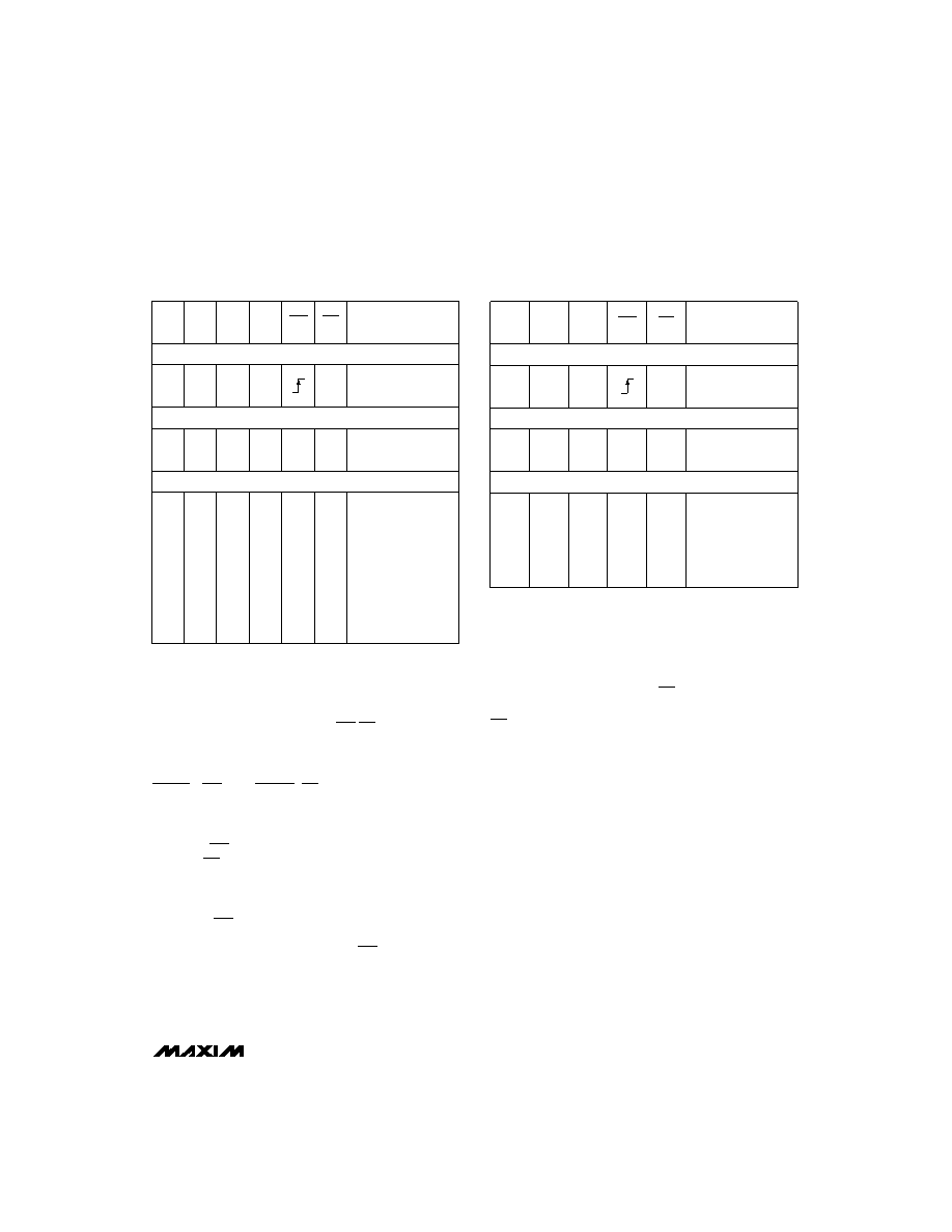
Table 1. DG528 Logic States
Table 2. DG529 Logic States
A2
A1
A0
EN
WR
RS
ON SWITCH
Latching
X
1
Maintains previous
switch condition
Reset
X
0
None
(latches cleared)
Transparent Operation
X
0
1
X
0
1
0
1
X
0
1
0
1
0
1
0
1
0
1
0
1
None
1
2
3
4
5
6
7
8
A1
A0
EN
WR
RS
ON SWITCH
X
1
Maintains previous
switch condition
X
0
None
(latches cleared)
X
0
1
X
0
1
0
1
0
1
0
1
None
1
2
3
4
Latching
Reset
Transparent Operation
Note: Logic “1”: VAH ≥ 2.4V, Logic “0”: VAL ≤ 0.8V.
相关PDF资料 |
PDF描述 |
|---|---|
| VE-B2Y-IY-F2 | CONVERTER MOD DC/DC 3.3V 33W |
| MAX309CUE+T | IC MULTIPLEXER 4X1 16TSSOP |
| MAX308CUE+T | IC MULTIPLEXER 8X1 16TSSOP |
| VE-B2Y-IX-F3 | CONVERTER MOD DC/DC 3.3V 49.5W |
| MAX339CEE+ | IC MULTIPLEXER DUAL 4X1 16QSOP |
相关代理商/技术参数 |
参数描述 |
|---|---|
| DG528CCWN+ | 功能描述:多路器开关 IC 8:1 CMOS Mid Voltage Latchable MUX RoHS:否 制造商:Texas Instruments 通道数量:1 开关数量:4 开启电阻(最大值):7 Ohms 开启时间(最大值): 关闭时间(最大值): 传播延迟时间:0.25 ns 工作电源电压:2.3 V to 3.6 V 工作电源电流: 最大工作温度:+ 85 C 安装风格:SMD/SMT 封装 / 箱体:UQFN-16 |
| DG528CJ | 功能描述:多路器开关 IC RoHS:否 制造商:Texas Instruments 通道数量:1 开关数量:4 开启电阻(最大值):7 Ohms 开启时间(最大值): 关闭时间(最大值): 传播延迟时间:0.25 ns 工作电源电压:2.3 V to 3.6 V 工作电源电流: 最大工作温度:+ 85 C 安装风格:SMD/SMT 封装 / 箱体:UQFN-16 |
| DG528CJ+ | 功能描述:多路器开关 IC 8:1 CMOS Mid Voltage Latchable MUX RoHS:否 制造商:Texas Instruments 通道数量:1 开关数量:4 开启电阻(最大值):7 Ohms 开启时间(最大值): 关闭时间(最大值): 传播延迟时间:0.25 ns 工作电源电压:2.3 V to 3.6 V 工作电源电流: 最大工作温度:+ 85 C 安装风格:SMD/SMT 封装 / 箱体:UQFN-16 |
| DG528CK | 功能描述:多路器开关 IC RoHS:否 制造商:Texas Instruments 通道数量:1 开关数量:4 开启电阻(最大值):7 Ohms 开启时间(最大值): 关闭时间(最大值): 传播延迟时间:0.25 ns 工作电源电压:2.3 V to 3.6 V 工作电源电流: 最大工作温度:+ 85 C 安装风格:SMD/SMT 封装 / 箱体:UQFN-16 |
| DG528CWN | 功能描述:多路器开关 IC RoHS:否 制造商:Texas Instruments 通道数量:1 开关数量:4 开启电阻(最大值):7 Ohms 开启时间(最大值): 关闭时间(最大值): 传播延迟时间:0.25 ns 工作电源电压:2.3 V to 3.6 V 工作电源电流: 最大工作温度:+ 85 C 安装风格:SMD/SMT 封装 / 箱体:UQFN-16 |
发布紧急采购,3分钟左右您将得到回复。