- 您现在的位置:买卖IC网 > PDF目录381709 > DG9053 (Vishay Intertechnology,Inc.) Precision 8-Ch/Dual 4-Ch/Triple 2-Ch Low Voltage Analog Switches/Multiplexers PDF资料下载
参数资料
| 型号: | DG9053 |
| 厂商: | Vishay Intertechnology,Inc. |
| 英文描述: | Precision 8-Ch/Dual 4-Ch/Triple 2-Ch Low Voltage Analog Switches/Multiplexers |
| 中文描述: | 精密8-Ch/Dual 4-Ch/Triple 2通道低电压模拟开关/多路复用器 |
| 文件页数: | 6/12页 |
| 文件大小: | 178K |
| 代理商: | DG9053 |
www.vishay.com
6
Document Number: 73410
S-52072-Rev. A, 10-Oct-05
Vishay Siliconix
DG9051/9052/9053
New Product
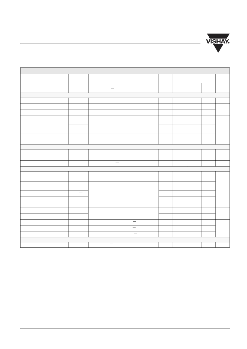
Notes
a. Leakage parameters are guaranteed by worst case test condition and not subject to production test.
b. Room = 25°C, Full = as determined by the operating temperature suffix.
c. The algebraic convention whereby the most negative value is a minimum and the most positive a maximum, is used in this data sheet.
d. Typical values are for DESIGN AID ONLY, not guaranteed nor subject to production testing.
e. Guaranteed by design, not subject to production test.
f. V
IN
= input voltage to perform proper function.
g.
r
DON
= r
DON
Max – r
DON
Min.
h. Worst case isolation occurs on Channel 4 due to proximity to the drain pin.
i. r
DON
flatness is measured as the difference between the minimum and maximum measured values across a defined Analog signal.
Stresses beyond those listed under “Absolute Maximum Ratings” may cause permanent damage to the device. These are stress ratings only, and functional operation
of the device at these or any other conditions beyond those indicated in the operational sections of the specifications is not implied. Exposure to absolute maximum
rating conditions for extended periods may affect device reliability.
SPECIFICATIONS (SINGLE SUPPLY 3 V)
Parameter
Symbol
Test Condition
Otherwise Unless Specified
V+ = 3 V, ±10 %, V– = 0 V
V
EN
= 0.4 V or 2.0 V
Temp
b
Limits
–40 to 85°C
Unit
Min
c
Typ
d
Max
c
Analog Switch
Analog Signal Range
e
On-Resistance
r
ON
Match Between Channels
g
V
ANALOG
r
ON
r
ON
Full
0
3
V
V+ = 2.7 V, V
D
= 1.5 V, I
S
= 0.1 mA
V+ = 2.7 V, V
D
= 1.5 V, I
S
= 0.1 mA
Room
Room
130
12
Switch Off Leakage Current
a
I
S(off)
V+ = 3.3 V, V
EN
= 2.0 V
V
S
= 3 or 0.3 V, V
D
= 0.3 or 3 V
Room
Full
Room
Full
–1
–20
–1
–20
1
20
1
20
nA
I
D(off)
Channel On Leakage Current
a
I
D(on)
V+ = 3.3 V, V
EN
= 0 V
V
S
= 3 or 0.3 V, V
D
= 0.3 or 3 V
Room
Full
–2
–10
2
10
Digital Control
Logic High Input Voltage
V
INH
V
INL
I
IN
Full
2.0
V
Logic Low Input Voltage
Full
0.4
Input Current
a
Dynamic Characteristics
V
AX
= V
EN
= 2.0 V or 0.4 V
Full
–1
1
μA
Transition Time
t
TRANS
V+ = 2.7 V, V
NO/NC
= 1.5 V/0 V, 0 V/1.5 V
R
L
= 300
, C
L
= 35 pF
Room
80
ns
Break-Before-Make Time
t
BBM
V+ = 2.7 V, V
X,Y, Z
= 1.5 V, V
S
= 0 V,
R
L
= 300
, C
L
= 35 pF
Room
Full
Room
5
25
Enable Turn-On Time
t
ON(EN)
t
OFF(EN)
Q
90
Enable Turn-Off Time
Charge Injection
e
Off-Isolation
e,h
Crosstalk
e
Source Off Capacitance
e
Drain Off Capacitance
e
Drain On Capacitance
e
Power Supply
Power Supply Current
Room
Room
30
C
L
= 1 nF, V
GEN
= 0 V, R
GEN
= 0
9
pC
OIRR
f = 1 MHz, R
L
= 50
Room
–78
dB
X
TALK
C
S(off)
C
D(off)
C
D(on)
Room
–83
f = 1 MHz, V
S
= 0 V, V
EN
= 1.8 V
f = 1 MHz, V
D
= 0 V, V
EN
= 1.8 V
f = 1 MHz, V
D
= 0 V, V
EN
= 0 V
Room
5
pF
Room
10
Room
15
I+
V
EN
= V
A
= 0 V or V+
Room
1.0
μA
相关PDF资料 |
PDF描述 |
|---|---|
| DG9053DQ-T1-E3 | Precision 8-Ch/Dual 4-Ch/Triple 2-Ch Low Voltage Analog Switches/Multiplexers |
| DG9232 | Low-Voltage Dual SPST Analog Switch |
| DG9232DQ | Low-Voltage Dual SPST Analog Switch |
| DG9232DY | Low-Voltage Dual SPST Analog Switch |
| DG9233 | Low-Voltage Dual SPST Analog Switch |
相关代理商/技术参数 |
参数描述 |
|---|---|
| DG9053DQ-T1-E3 | 功能描述:模拟开关 IC Triple 2-Ch SPDT RoHS:否 制造商:Texas Instruments 开关数量:2 开关配置:SPDT 开启电阻(最大值):0.1 Ohms 切换电压(最大): 开启时间(最大值): 关闭时间(最大值): 工作电源电压:2.7 V to 4.5 V 最大工作温度:+ 85 C 安装风格:SMD/SMT 封装 / 箱体:DSBGA-16 |
| DG908AK | 制造商:未知厂家 制造商全称:未知厂家 功能描述:8-Channel Analog Multiplexer |
| DG908DJ | 制造商:未知厂家 制造商全称:未知厂家 功能描述:8-Channel Analog Multiplexer |
| DG909AK | 制造商:未知厂家 制造商全称:未知厂家 功能描述:4-Channel Analog Multiplexer |
| DG909DJ | 制造商:未知厂家 制造商全称:未知厂家 功能描述:4-Channel Analog Multiplexer |
发布紧急采购,3分钟左右您将得到回复。