- 您现在的位置:买卖IC网 > PDF目录18748 > DNT24P (RFM)RF TXRX 2.4GHZ ISM U.FL PDF资料下载
参数资料
| 型号: | DNT24P |
| 厂商: | RFM |
| 文件页数: | 4/8页 |
| 文件大小: | 0K |
| 描述: | RF TXRX 2.4GHZ ISM U.FL |
| 产品培训模块: | Frequency Hopping Spread Spectrum Portfolio Overview |
| 标准包装: | 20 |
| 频率: | 2.4GHz |
| 数据传输率 - 最大: | 250kbps |
| 调制或协议: | FHSS,FSK |
| 应用: | ISM |
| 功率 - 输出: | 63mW |
| 灵敏度: | -100dBm |
| 电源电压: | 3.3 V ~ 5.5 V |
| 电流 - 接收: | 110mA |
| 电流 - 传输: | 170mA |
| 数据接口: | 连接器 |
| 天线连接器: | U.FL |
| 工作温度: | -40°C ~ 85°C |
| 封装/外壳: | 模块 |
| 包装: | 托盘 |
| 其它名称: | 583-1163 |
��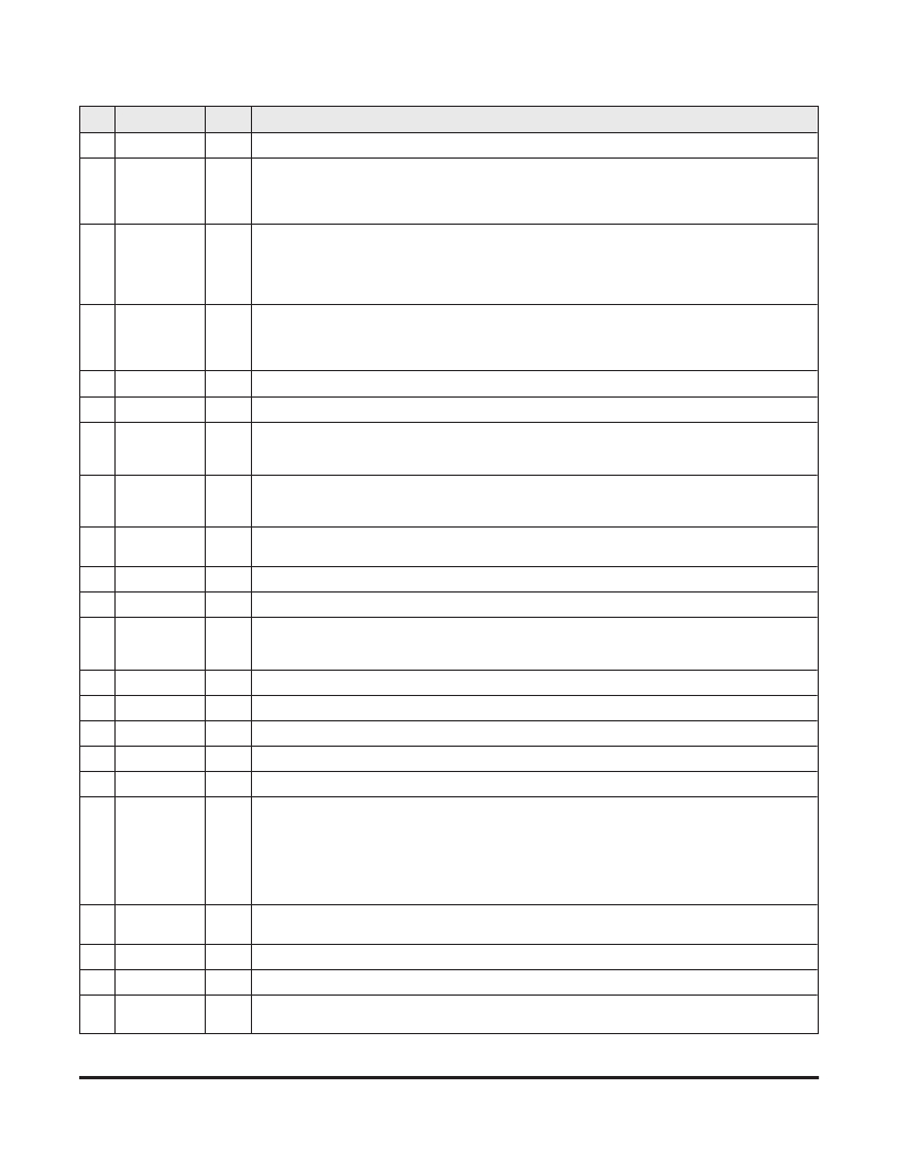 �
�
�DNT24� I/O� Descriptions�
�Pin�
�1�
�Name�
�GND�
�I/O�
�-�
�Description�
�Power� supply� and� signal� ground.� Connect� to� the� host� circuit� board� ground.�
�This� pin’s� default� configuration� is� data� activity� output.� On� a� base,� this� signal� blinks� when� a� valid� packet� is�
�2�
�ACT�
�(DIAG_TX)�
�O�
�(O)�
�received.� On� a� remote,� this� signal� blinks� when� a� packet� is� transmitted.� On� a� router,� this� signal� blinks� when�
�a� valid� upstream� packet� is� received� or� a� downstream� packet� is� transmitted.� Alternate� pin� function� is� the� di-�
�agnostic� serial� port� output.�
�This� pin’s� default� configuration� is� data� carrier� detect� output.� On� a� base,� this� signal� is� asserted� when� any�
�3�
�/DCD�
�(DIAG_RX)�
�O�
�(I)�
�valid� packet� is� received,� and� is� cleared� if� no� packets� are� heard� for� the� configured� router/remote� registra-�
�tion� time-out� interval.� On� a� router� or� remote,� this� signal� is� asserted� when� the� radio� obtains� hopping� pattern�
�synchronization,� and� remains� asserted� until� no� beacons� are� heard� for� 50� hops.� Alternate� pin� function� is�
�the� diagnostic� serial� port� input.�
�Configurable� digital� I/O� port� 0.� When� configured� as� an� input,� an� internal� pull-up� resistor� can� be� selected�
�4�
�GPIO0�
�I/O�
�and� direct� interrupt� from� sleep� can� be� invoked.� When� configured� as� an� output,� the� power-on� state� is�
�configurable.� In� sleep� mode� the� pin� direction,� input� pull-up� selection� or� output� state� are� also� separately�
�configurable.�
�5�
�6�
�7�
�8�
�9�
�10�
�11�
�12�
�13�
�14�
�15�
�16�
�17�
�RADIO_TXD�
�RADIO_RXD�
�GPOI4�
�(/HOST_CTS)�
�GPOI5�
�(� /HOST_RTS)�
�DAC0�
�GPIO2�
�GPIO1�
�GPIO3�
�(DAV)�
�DAC1�
�VCC�
�GND�
�GND�
�/RESET�
�O�
�I�
�I/O�
�(O)�
�I/O�
�(I)�
�O�
�I/O�
�I/O�
�I/O�
�(O)�
�O�
�I�
�-�
�-�
�I�
�Serial� data� output� from� the� radio.�
�Serial� data� input� to� the� radio.�
�Default� pin� function� is� GPIO4� with� the� same� configuration� options� as� GPIO0.� Alternate� pin� function� is�
�UART/SPI� flow� control� output.� The� module� sets� this� line� low� when� it� is� ready� to� accept� data� from� the� host�
�on� the� RADIO_RXD� or� MOSI� input.� When� the� line� goes� high,� the� host� must� stop� sending� data.�
�Default� pin� function� is� GPIO5� with� the� same� configuration� options� as� GPIO0.� Alternate� pin� function� is�
�UART/SPI� flow� control� input.� The� host� sets� this� line� low� to� allow� data� to� flow� from� the� module� on�
�the� RADIO_TXD� pin.� When� the� host� sets� this� line� high,� the� module� will� stop� sending� data� to� the� host.�
�12-bit� DAC� 0� output.� Full� scale� output� can� be� referenced� to� the� voltage� at� pin� 25� or� the� 3.3� V� regulated�
�module� bus� voltage.�
�Configurable� digital� I/O� port� 2.� Same� configuration� options� as� GPIO0.�
�Configurable� digital� I/O� port� 1.� Same� configuration� options� as� GPIO0.�
�Default� pin� function� is� GPIO3� with� the� same� configur� ation� options� as� GPIO0.� When� SPI� slave� mode� oper-�
�ation� is� enabled,� a� logic� high� on� this� pin� indicates� when� data� is� available� to� be� clocked� out� by� the� SPI�
�master.�
�12-bit� DAC� 1� output.� Same� specifications� and� configuration� options� as� DAC0.�
�Power� supply� input,� +3.3� to� +5.5� Vdc.�
�Power� supply� and� signal� ground.� Connect� to� the� host� circuit� board� ground.�
�Power� supply� and� signal� ground.� Connect� to� the� host� circuit� board� ground.�
�Active� low� module� hardware� reset.�
�ADC� input� 0.� This� pin� is� a� direct� ADC� input� when� the� ADC� is� operating� in� single-ended� mode,� or� the� differ-�
�ential� negative� input� for� positive� inputs� applied� to� ADC1� or� ADC2� when� the� ADC� is� operating� in� differential�
�mode.� Full-scale� reading� can� be� referenced� to� Pin� 25� for� ratiometric� measurements.� For� absolute� mea-�
�18�
�ADC0�
�I�
�surements,� the� ADC� can� use� either� the� regulated� supply� voltage� divided� by� 1.6� (about� 2.06� V),� or� an� ex-�
�ternal� voltage� applied� to� Pin� 25.� In� single-ended� mode,� ADC� measurements� are� 11-bit� unsigned� values�
�with� full� scale� nominally� 2.7� V� when� referenced� to� a� 2.7� V� input� on� Pin� 27.� In� differential� mode,� ADC� mea-�
�surements� are� 12-bit� signed� values.�
�19�
�20�
�21�
�22�
�ADC1�
�MISO�
�MOSI�
�/SS�
�I�
�I/O�
�I/O�
�I/O�
�ADC� input� 1.� Direct� input� when� the� ADC� is� operating� in� single-ended� mode,� positive� differential� input� rela-�
�tive� to� ADC0� when� the� ADC� is� operating� in� differential� mode.�
�This� pin� is� the� SPI� master� mode� input� or� slave� mode� output.�
�This� pin� is� the� SPI� master� mode� output� or� slave� mode� input.�
�SPI� active� low� slave� select.� This� pin� is� an� output� when� the� module� is� operating� as� a� master,� and� an� input�
�when� it� is� operating� as� a� slave.�
�www.RFM.com� E-mail:� info@rfm.com�
�?� 2011-2012� by� RF� Monolithics,� Inc.�
�Page� 4� of� 7�
�DNT24� -� 08/01/12�
�相关PDF资料 |
PDF描述 |
|---|---|
| IF-24-24 | XFRMR 115/230V 12V 2A 24VA PCB |
| XBP24BZ7UITB003 | MODULE ZIGBEE-PRO W/U.FL ANT |
| IF-24-20 | XFRMR 115/230V 10V 2.4A 24VA PCB |
| IF-24-16 | XFRMR 115/230V 8V 3A 24VA PCB |
| IF-24-12 | XFRMR 115/230V 6V 4A 24VA PCB |
相关代理商/技术参数 |
参数描述 |
|---|---|
| DNT24PA | 功能描述:射频模块 2.4 GHz 10 and 63mW 128 Bit AES RoHS:否 制造商:Linx Technologies 产品:Transceiver Modules 频带:902 MHz to 928 MHz 输出功率:- 15.5 dBm to + 12.5 dBm 接口类型:UART 工作电源电压:- 0.3 VDC to + 5.5 VDC 传输供电电流:38.1 mA 接收供电电流:22.7 mA 天线连接器类型:U.FL 最大工作温度:+ 85 C 尺寸:1.15 mm x 0.63 mm x 0.131 mm |
| DNT25SX | 制造商:CEEP 功能描述:SOCKET D T&D 25WAY |
| DNT37SX | 制造商:CEEP 功能描述:SOCKET D T&D 37 WAY |
| DNT50SX | 制造商:CEEP 功能描述:SOCKET D T&D 50WAY |
| DNT625S/M | 制造商:Denon Electronics 功能描述:SERVICE MANUAL |
发布紧急采购,3分钟左右您将得到回复。