- 您现在的位置:买卖IC网 > PDF目录223665 > DR-11525DX-585 (DATA DEVICE CORP) DIGITAL TO SYNCHRO OR RESOLVER, CDIP36 PDF资料下载
参数资料
| 型号: | DR-11525DX-585 |
| 厂商: | DATA DEVICE CORP |
| 元件分类: | 位置变换器 |
| 英文描述: | DIGITAL TO SYNCHRO OR RESOLVER, CDIP36 |
| 封装: | 0.780 X 1.900 INCH, 0.210 INCH HEIGHT, CERAMIC, DDIP-36 |
| 文件页数: | 5/8页 |
| 文件大小: | 155K |
| 代理商: | DR-11525DX-585 |
5
Data Device Corporation
www.ddc-web.com
DR-11525
G-06/05-0
The reference conditioner output -R is intended for test purpos-
es. For a 26 Vrms nominal input to RH, RL, -R should be 5.9
Vrms.
The timing relationship of LL, LM, and LA is shown in FIGURE 2
as a design reference.
OUTPUT SCALING AND REF. LEVEL ADJUSTMENT
The DR-11525 operates like a multiplying D/A converter in that
the voltage of each output line is directly proportional to the ref-
erence voltage. See FIGURE 3.
The magnitude of the resistors, R', in ohms is calculated as fol-
lows:
*Note: For RH2, RL2 and RH3, RL3: Vout(single-ended) = 1/2 VoutL-L.
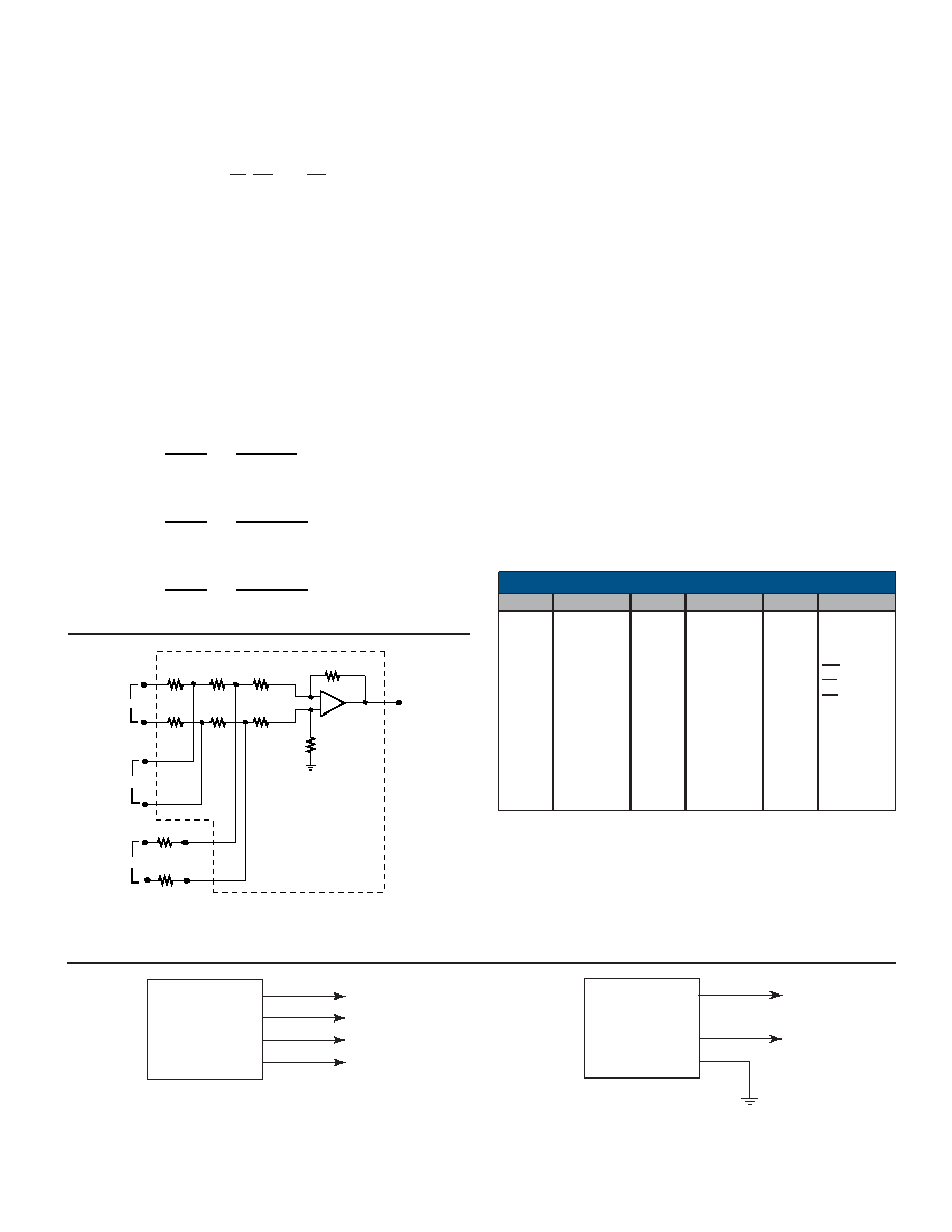
FIGURE 4. DIFFERENTIAL RESOLVER OUTPUT
FIGURE 5. SINGLE-ENDED RESOLVER OUTPUT
TABLE 3. PIN CONNECTION TABLE
PIN
NAME
13
14
15
16
17
18
19
20
21
22
23
24
NC
+15V
GND
-15V
RH2 (6.81V)
RL2 (6.81V)
-R
RL (11.8V)
RL3 (2V)
RH (11.8V)
RH3 (2V)
Bit 14
1
2
3
4
5
6
7
8
9
10
11
12
Bit 13
Bit 12
Bit 11
Bit 10
Bit 9
Bit 8
Bit 7
Bit 6
Bit 5
Bit 4
Bit 3
Bit 2
25
26
27
28
29
30
31
32
33
34
35
36
Bit 1 (MSB)
Bit 15
Bit 16 (LSB)
LM
LL
LA
S4 (-COS)
S1 (-SIN)
NC
S3 (+SIN)
S2 (+COS)
Notes:
1. -R (Pin 7) can be used for test purposes to detect whether a reference signal
is present. See block diagram.
2. Functions LL, LA, and LM may be left unconnected when not used.
3. External scaling resistor pin 11 RH3 output pins (31, 32, 35, 36).
4. RH and RL (pins 10, 8) 26 V reference with differential outputs on pins 35, 36,
32, 31.
5. RH2 and RL2 (pins 5, 6) 26 V reference with single-ended output on pins 35,
36.
6. RH3 and RL3 (pins 11, 9) 4.4 V reference with single-ended outputs on pins
35, 36.
FIGURE 3. REFERENCE LEVEL ADJUSTMENT
49.92k
36.71k
13.37k
REFERENCE
INPUTS
V (RH-RL)
V (RH2-RL2)
V (RH3-RL3)
8.703k
45.38k
VOUT L-L
+
_
R
′
R
′
*Changing input volt, will scale down output volt
1) 26V
2) 26V
3) 4.4V
1) 11.8V Nom
2) 6.8V Single Ended
3) 2.0V Nom
OUTPUT PHASING AND OUTPUT SCALE FACTOR
The analog output signals have the following phasing:
Resolver output:
S3—S1 = (RH - RL)Ao(1 + A(
θ)) sin θ
S2—S4 = (RH - RL)Ao(1 + A(
θ)) cos θ
The output amplifiers simultaneously track reference voltage
fluctuations because they are proportional to (RH - RL). The
transformation ratio Ao is 11.8/26 for 11.8 VrmsL-L output. The
maximum variation in Ao from all causes is ± 0.2%. The term
A(
θ) represents the variation of the amplitude with the digital sig-
nal input angle. A(
θ), which is called the scale factor variation, is
a smooth function of (
θ) without discontinuities and is less than
±0.1% for all values of (
θ). Therefore, the analog output can vary
as much as ±0.3% due to the transformation ratio and scale fac-
tor variations.
Because the amplitude factor (RH - RL)Ao(1 + A(
θ)) varies
simultaneously on all output lines, it will not be a source of error
when the DR-11525 is to drive a ratiometric system such as a
synchro or resolver. However, if the outputs are used indepen-
dently, as in x-y plotters, the amplitude variations must be taken
into account.
For RH-RL:
VoutL-L
=
45.38k
Vin
100k + R'
*For RH2-RL2: VoutL-L
=
45.38k
Vin
86.63k + R'
*For RH3-RL3: VoutL-L
=
45.38k
Vin
49.92k + R'
DR-11525
S3
S1
S2
S4
S3
S1
S2
S4
35
32
36
31
DR-11525
S3
S2
GND
S3
S2
35
(+SIN)
36
(+COS)
3
相关PDF资料 |
PDF描述 |
|---|---|
| DR-11525DX-594 | DIGITAL TO SYNCHRO OR RESOLVER, CDIP36 |
| DR-11525DX-414K | DIGITAL TO SYNCHRO OR RESOLVER, CDIP36 |
| DR-11525DX-424S | DIGITAL TO SYNCHRO OR RESOLVER, CDIP36 |
| DR-11525DX-325L | DIGITAL TO SYNCHRO OR RESOLVER, CDIP36 |
| DR-11525DX-354S | DIGITAL TO SYNCHRO OR RESOLVER, CDIP36 |
相关代理商/技术参数 |
参数描述 |
|---|---|
| DR-11525DX803 | 制造商:未知厂家 制造商全称:未知厂家 功能描述:Converter |
| DR-11525DX804 | 制造商:未知厂家 制造商全称:未知厂家 功能描述:Converter |
| DR-11525DX805 | 制造商:未知厂家 制造商全称:未知厂家 功能描述:Converter |
| DR-11525DX813 | 制造商:未知厂家 制造商全称:未知厂家 功能描述:Converter |
| DR-11525DX814 | 制造商:未知厂家 制造商全称:未知厂家 功能描述:Converter |
发布紧急采购,3分钟左右您将得到回复。