- 您现在的位置:买卖IC网 > Datasheet目录409 > DR-TXC100-433 (RFM)BOARD EVALUATION 433MHZ TXC100 Datasheet资料下载
参数资料
| 型号: | DR-TXC100-433 |
| 厂商: | RFM |
| 文件页数: | 3/11页 |
| 文件大小: | 0K |
| 描述: | BOARD EVALUATION 433MHZ TXC100 |
| 标准包装: | 1 |
| 类型: | 发射器,ASK,FSK |
| 频率: | 433.92MHz |
| 适用于相关产品: | TXC100 |
| 已供物品: | 板 |
�� �
�
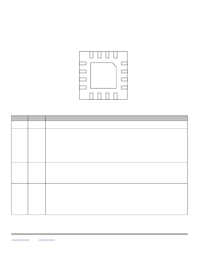
�Pin� Configuration�
�BOTTOM� VIEW�
�3x3mm�
�13�
�14�
�15�
�16�
�Dev1�
�Dev0�
�Clk1�
�Clk0�
�12�
�11�
�10�
�9�
�1�
�2�
�3�
�4�
�V� DD�
�Mode� Sel�
�Data� IN�
�Stdby�
�8�
�7�
�6�
�5�
�Pin� Description�
�Pin�
�1�
�2�
�3�
�4�
�Name�
�V� DD�
�Mode� Sel�
�Data� IN�
�Stdby�
�Description�
�V� DD� is� the� supply� voltage� for� the� PLL� and� logic� circuitry.� Bypass� this� pin� as� close� as� possible� with� parallel� 1.0� μF,� 0.01� μF,� 220� pF�
�capacitors.�
�The� Mode� Select� Pin� allows� the� TXC100� to� be� set� in� either� OOK/ASK� or� FSK� mode:�
�Logic� Low:� OOK/ASK� mode�
�Logic� High:� FSK� mode�
�In� OOK/ASK� mode,� data� input� to� the� Data� IN� Pin� (3)� gates� the� internal� power� amplifier.� A� logic� high� turns� the� power� amplifier� on.� A� logic�
�low� turns� off� the� power� amplifier.�
�In� FSK� mode,� data� input� to� the� Data� IN� Pin� shifts� the� carrier� frequency� by� the� amount� programmed� through� the� DEV[2..0]� pins� (11,12,13).�
�A� logic� low� performs� no� shift.� The� frequency� of� a� logic� low� input� in� FSK� mode� is� the� same� frequency� as� a� logic� high� in� OOK/ASK� mode.�
�The� FSK� deviation� is� achieved� by� pulling� the� crystal� frequency.� See� Crystal� Reference� section� (pin� 15)� for� more� details.� The� maximum�
�FSK� deviation� for� the� 315� MHz� band� and� 433� MHz� band� is� approximately� 55� kHz� and� 80� kHz,� respectively.�
�The� Data� Input� Pin� turns� the� Power� Amplifier� on/off� in� OOK/ASK� mode,� or� high/low� frequency� in� FSK� mode:�
�Low� (OOK/ASK� mode):� Power� Amplifier� off�
�High� (OOK/ASK� mode):� Power� Amplifier� on�
�Low� (FSK� mode):� Low� frequency�
�High� (FSK� mode):� High� frequency�
�The� Standby� Input� Pin� selects� active� or� low� power� shutdown/standby� mode:�
�If� this� pin� unconnected� or� logic� low,� the� TXC100� is� placed� in� low� current� standby� mode.�
�If� this� pin� is� logic� high,� the� TXC100� is� in� active� mode� and� ready� to� transmit�
�Note:� Lowest� current� consumption� is� achieved� when� all� configuration� pins� are� logic� low.�
�When� this� pin� sets� the� device� in� low� power� shutdown,� the� device� draws� nominally� 0.2� nA.� When� the� device� is� brought� out� of� standby� with�
�a� logic� high� input,� it� is� ready� for� operation� within� 200� μs.� This� pin� has� an� internal� pull-down� resistor� so� it� can� be� pulled� low� or� left�
�unconnected.The� 200� μs� turn-on� time� is� due� to� crystal� start-up.� An� optimally� matched� crystal� will� minimize� this� turn-on� time.� See� the�
�Crystal� Reference� section� (Pin� 15)� for� details� on� crystal� load� matching.�
�www.RFM.com� Email:� info@rfm.com�
�?RF� Monolithics,� Inc.�
�Page� 3� of� 11�
�TXC100� -� 08/18/10�
�相关PDF资料 |
PDF描述 |
|---|---|
| DR-WLS1273L-EV | KIT EVAL FOR WLS1273L |
| DR7000-DK | 3G DEVELOPMENT KIT 433.92MHZ |
| DR7001-DK | 3G DEVELOPMENT KIT 315 MHZ |
| DR7003-DK | 3G DEVELOPMENT KIT 303.825 MHZ |
| DR8000-DK | 3G DEVELOPMENT KIT 916MHZ |
相关代理商/技术参数 |
参数描述 |
|---|---|
| DR-TXC101-315-DK | 功能描述:射频开发工具 TXC101 Development Kit 310-319 MHz RoHS:否 制造商:Taiyo Yuden 产品:Wireless Modules 类型:Wireless Audio 工具用于评估:WYSAAVDX7 频率: 工作电源电压:3.4 V to 5.5 V |
| DR-TXC102-433-DK | 功能描述:射频开发工具 TXC102 Development Kit 430-439 MHz RoHS:否 制造商:Taiyo Yuden 产品:Wireless Modules 类型:Wireless Audio 工具用于评估:WYSAAVDX7 频率: 工作电源电压:3.4 V to 5.5 V |
| DR-TXC102-868-DK | 功能描述:射频开发工具 TXC102 Development Kit 860-879 MHz RoHS:否 制造商:Taiyo Yuden 产品:Wireless Modules 类型:Wireless Audio 工具用于评估:WYSAAVDX7 频率: 工作电源电压:3.4 V to 5.5 V |
| DR-TXC102-915-DK | 功能描述:射频开发工具 TXC102 Development Kit 900-929 MHz RoHS:否 制造商:Taiyo Yuden 产品:Wireless Modules 类型:Wireless Audio 工具用于评估:WYSAAVDX7 频率: 工作电源电压:3.4 V to 5.5 V |
| DRU20R103KA | 制造商:Alpha 3 Manufacturing 功能描述: |
发布紧急采购,3分钟左右您将得到回复。