- 您现在的位置:买卖IC网 > PDF目录8916 > DS1086LU-B66+ (Maxim Integrated Products)IC ECONOSILL 3.3V SS 8-USOP PDF资料下载
参数资料
| 型号: | DS1086LU-B66+ |
| 厂商: | Maxim Integrated Products |
| 文件页数: | 13/17页 |
| 文件大小: | 0K |
| 描述: | IC ECONOSILL 3.3V SS 8-USOP |
| 其它有关文件: | Automotive Product Guide |
| 产品培训模块: | Lead (SnPb) Finish for COTS Obsolescence Mitigation Program |
| 标准包装: | 50 |
| 系列: | EconOscillator™ |
| 类型: | 扩展频谱时钟发生器 |
| PLL: | 无 |
| 输入: | 时钟 |
| 输出: | 时钟 |
| 电路数: | 1 |
| 比率 - 输入:输出: | 2:1 |
| 差分 - 输入:输出: | 无/无 |
| 除法器/乘法器: | 是/无 |
| 电源电压: | 2.7 V ~ 3.6 V |
| 工作温度: | -40°C ~ 85°C |
| 安装类型: | 表面贴装 |
| 封装/外壳: | 8-TSSOP,8-MSOP(0.118",3.00mm 宽) |
| 供应商设备封装: | 8-uMAX |
| 包装: | 管件 |
3.3V Spread-Spectrum EconOscillator
Maxim Integrated
5
DS1086L
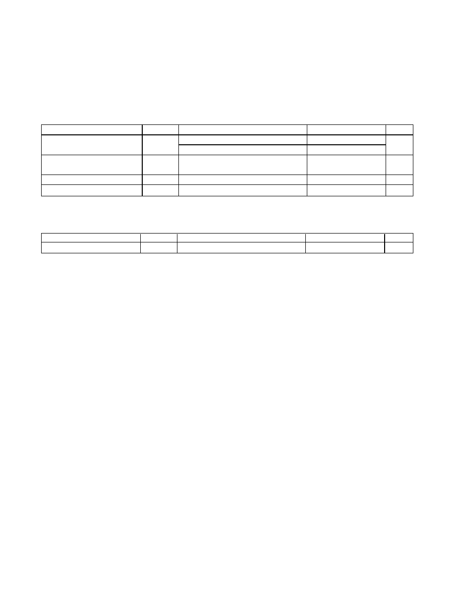
AC ELECTRICAL CHARACTERISTICS—2-WIRE INTERFACE (continued)
(VCC = 2.7V to 3.6V, TA = -40°C to +85°C.)
PARAMETER
SYMBOL
CONDITIONS
MIN
TYP
MAX
UNITS
Fast mode
0.6
Setup Time for STOP
tSU:STO
Standard mode
4.0
μs
Capacitive Load for Each Bus
Line
CB
(Note 16)
400
pF
EEPROM Write Cycle Time
tWR
10
ms
Input Capacitance
CI
5pF
NONVOLATILE MEMORY CHARACTERISTICS
(VCC = 2.7V to 3.6V)
PARAMETER
SYMBOL
CONDITIONS
MIN
TYP
MAX
UNITS
EEPROM Writes
+70°C
10,000
Note 1:
All voltages are referenced to ground.
Note 2:
DAC and OFFSET register settings must be configured to maintain the master oscillator frequency within this range.
Correct operation of the device is not guaranteed if these limits are exceeded.
Note 3:
This is the absolute accuracy of the master oscillator frequency at the default settings.
Note 4:
This is the change that is observed in master oscillator frequency with changes in voltage from nominal voltage at
TA = +25°C.
Note 5:
This is the percentage frequency change from the +25°C frequency due to temperature at VCC = 3.3V. The maximum temper-
ature change varies with the master oscillator frequency setting. The minimum occurs at the default master oscillator frequen-
cy (fdefault). The maximum occurs at the extremes of the master oscillator frequency range (33.3MHz or 66.6MHz).
Note 6:
The dither deviation of the master oscillator frequency is unidirectional and lower than the undithered frequency.
Note 7:
The integral nonlinearity of the frequency is a measure of the deviation from a straight line drawn between the two end-
points (fosc(MIN) to fosc(MAX)) of the range. The error is in percentage of the span.
Note 8:
This is true when the prescaler = 1.
Note 9:
Frequency settles faster for small changes in value. During a change, the frequency transitions smoothly from the original
value to the new value.
Note 10:
This indicates the time elapsed between power-up and the output becoming active. An on-chip delay is intentionally
introduced to allow the oscillator to stabilize. tstab is equivalent to approximately 512 master clock cycles and therefore
depends on the programmed clock frequency.
Note 11:
Output voltage swings can be impaired at high frequencies combined with high output loading.
Note 12:
A fast-mode device can be used in a standard-mode system, but the requirement tSU:DAT > 250ns must then be met.
This is automatically the case if the device does not stretch the LOW period of the SCL signal. If such a device does
stretch the LOW period of the SCL signal, it must output the next data bit to the SDA line at least tR MAX + tSU:DAT =
1000ns + 250ns = 1250ns before the SCL line is released.
Note 13:
After this period, the first clock pulse is generated.
Note 14:
A device must internally provide a hold time of at least 300ns for the SDA signal (referred to as the VIH MIN of the SCL
signal) to bridge the undefined region of the falling edge of SCL.
Note 15:
The maximum tHD:DAT need only be met if the device does not stretch the LOW period (tLOW) of the SCL signal.
Note 16:
CB—total capacitance of one bus line, timing referenced to 0.9 x VCC and 0.1 x VCC.
Note 17:
Typical frequency shift due to aging is ±0.5%. Aging stressing includes Level 1 moisture reflow preconditioning (24hr
+125°C bake, 168hr 85°C/85%RH moisture soak, and three solder reflow passes +240 +0/-5°C peak) followed by 1000hr
max VCC biased 125°C HTOL, 1000 temperature cycles at -55°C to +125°C, 96hr 130°C/85%RH/3.6V HAST and 168hr
121°C/2 ATM Steam/Unbiased Autoclave.
Note 18:
tstab is the time required after exiting power-down to the beginning of output oscillations. In addition, a delay of tDACstab
is required before the frequency will be within its specified tolerance.
相关PDF资料 |
PDF描述 |
|---|---|
| M83723/96G2041N | CONN PLUG 41POS STRAIGHT W/PINS |
| VE-J2Y-MZ-F3 | CONVERTER MOD DC/DC 3.3V 16.5W |
| MS27496E25B35SC | CONN RCPT 128POS BOX MNT W/SCKT |
| VE-J2X-MZ-F2 | CONVERTER MOD DC/DC 5.2V 25W |
| MS27496E25B35SB | CONN RCPT 128POS BOX MNT W/SCKT |
相关代理商/技术参数 |
参数描述 |
|---|---|
| DS1086LU-B66+ | 功能描述:可编程振荡器 3.3V Spread-Spectrum EconOscillator RoHS:否 制造商:IDT 封装 / 箱体:5 mm x 7 mm x 1.5 mm 频率:15.476 MHz to 866.67, 975 MHz to 1300 MHz 频率稳定性:+/- 50 PPM 电源电压:3.63 V 负载电容:10 pF 端接类型:SMD/SMT 输出格式:LVPECL 最小工作温度:- 40 C 最大工作温度:+ 85 C 尺寸:7 mm W x 5 mm L x 1.5 mm H 封装: |
| DS1086LU-B66+T | 功能描述:可编程振荡器 3.3V Spread-Spectrum EconOscillator RoHS:否 制造商:IDT 封装 / 箱体:5 mm x 7 mm x 1.5 mm 频率:15.476 MHz to 866.67, 975 MHz to 1300 MHz 频率稳定性:+/- 50 PPM 电源电压:3.63 V 负载电容:10 pF 端接类型:SMD/SMT 输出格式:LVPECL 最小工作温度:- 40 C 最大工作温度:+ 85 C 尺寸:7 mm W x 5 mm L x 1.5 mm H 封装: |
| DS1086LU-C01+ | 功能描述:可编程振荡器 3.3V Spread-Spectrum EconOscillator RoHS:否 制造商:IDT 封装 / 箱体:5 mm x 7 mm x 1.5 mm 频率:15.476 MHz to 866.67, 975 MHz to 1300 MHz 频率稳定性:+/- 50 PPM 电源电压:3.63 V 负载电容:10 pF 端接类型:SMD/SMT 输出格式:LVPECL 最小工作温度:- 40 C 最大工作温度:+ 85 C 尺寸:7 mm W x 5 mm L x 1.5 mm H 封装: |
| DS1086LU-C01+T | 功能描述:可编程振荡器 3.3V Spread-Spectrum EconOscillator RoHS:否 制造商:IDT 封装 / 箱体:5 mm x 7 mm x 1.5 mm 频率:15.476 MHz to 866.67, 975 MHz to 1300 MHz 频率稳定性:+/- 50 PPM 电源电压:3.63 V 负载电容:10 pF 端接类型:SMD/SMT 输出格式:LVPECL 最小工作温度:- 40 C 最大工作温度:+ 85 C 尺寸:7 mm W x 5 mm L x 1.5 mm H 封装: |
| DS1086LU-C02+ | 功能描述:可编程振荡器 3.3V Spread-Spectrum EconOscillator RoHS:否 制造商:IDT 封装 / 箱体:5 mm x 7 mm x 1.5 mm 频率:15.476 MHz to 866.67, 975 MHz to 1300 MHz 频率稳定性:+/- 50 PPM 电源电压:3.63 V 负载电容:10 pF 端接类型:SMD/SMT 输出格式:LVPECL 最小工作温度:- 40 C 最大工作温度:+ 85 C 尺寸:7 mm W x 5 mm L x 1.5 mm H 封装: |
发布紧急采购,3分钟左右您将得到回复。