- 您现在的位置:买卖IC网 > PDF目录2067 > DS1094LU-42M+ (Maxim Integrated Products)IC ECONOSCILLATOR SS 8-USOP PDF资料下载
参数资料
| 型号: | DS1094LU-42M+ |
| 厂商: | Maxim Integrated Products |
| 文件页数: | 11/11页 |
| 文件大小: | 0K |
| 描述: | IC ECONOSCILLATOR SS 8-USOP |
| 其它有关文件: | Automotive Product Guide |
| 产品培训模块: | Lead (SnPb) Finish for COTS Obsolescence Mitigation Program |
| 标准包装: | 50 |
| 系列: | EconOscillator™ |
| 类型: | 时钟发生器 |
| PLL: | 无 |
| 输入: | 时钟 |
| 输出: | 时钟 |
| 电路数: | 1 |
| 比率 - 输入:输出: | 2:4 |
| 差分 - 输入:输出: | 无/无 |
| 频率 - 最大: | 2MHz |
| 除法器/乘法器: | 是/无 |
| 电源电压: | 3 V ~ 3.6 V |
| 工作温度: | -40°C ~ 85°C |
| 安装类型: | 表面贴装 |
| 封装/外壳: | 8-TSSOP,8-MSOP(0.118",3.00mm 宽) |
| 供应商设备封装: | 8-uMAX |
| 包装: | 管件 |
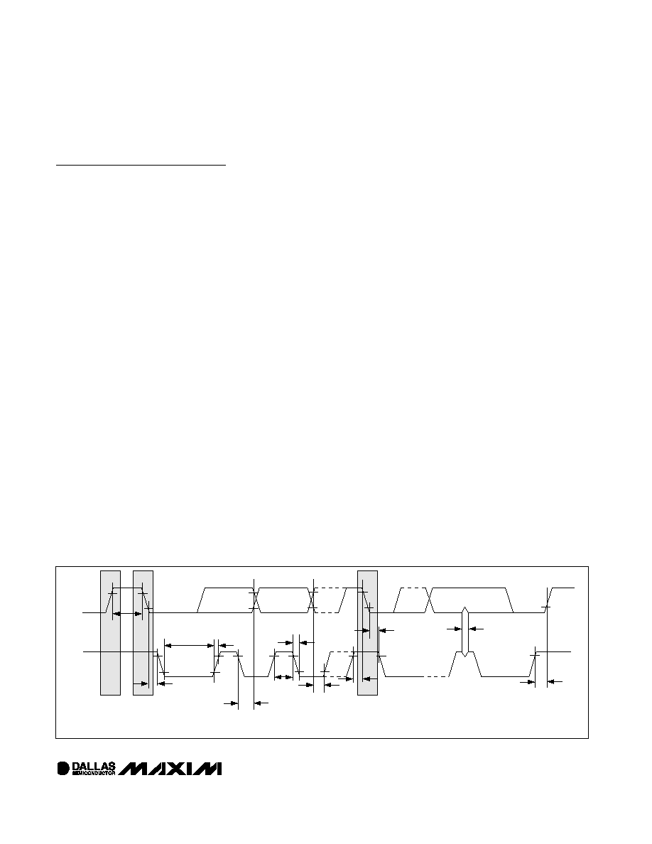
2-Wire Serial Interface
Description
Definitions
The following terminology is commonly used to
describe 2-wire data transfers.
Master Device: The master device controls the slave
devices on the bus. The master device generates SCL
clock pulses, start, and stop conditions.
Slave Devices: Slave devices send and receive data
at the master’s request.
Bus Idle or Not Busy: Time between stop and start
conditions when both SDA and SCL are inactive and in
their logic high states. When the bus is idle it often initi-
ates a low-power mode for slave devices.
Start Condition: A start condition is generated by the
master to initiate a new data transfer with a slave.
Transitioning SDA from high to low while SCL remains
high generates a start condition. See the timing dia-
gram for applicable timing.
Stop Condition: A stop condition is generated by the
master to end a data transfer with a slave. Transitioning
SDA from low to high while SCL remains high gener-
ates a stop condition. See the timing diagram for
applicable timing.
Repeated Start Condition: The master can use a
repeated start condition at the end of one data transfer
to indicate that it will immediately initiate a new data
transfer following the current one. Repeated starts are
commonly used during read operations to identify a
specific memory address to begin a data transfer. A
repeated start condition is issued identically to a nor-
mal start condition. See the timing diagram for applica-
ble timing.
Bit Write: Transitions of SDA must occur during the low
state of SCL. The data on SDA must remain valid and
unchanged during the entire high pulse of SCL plus the
setup and hold time requirements (see Figure 3). Data is
shifted into the device during the rising edge of the SCL.
Bit Read: At the end of a write operation, the master
must release the SDA bus line for the proper amount of
setup time (see Figure 3) before the next rising edge of
SCL during a bit read. The device shifts out each bit of
data on SDA at the falling edge of the previous SCL
pulse, and the data bit is valid at the rising edge of the
current SCL pulse. Remember that the master gener-
ates all SCL clock pulses including when it is reading
bits from the slave.
Acknowledgement
(ACK
and
NACK):
An
Acknowledgement (ACK) or Not Acknowledge (NACK) is
always the 9th bit transmitted during a byte transfer. The
device receiving data (the master during a read or the
slave during a write operation) performs an ACK by
transmitting a zero during the 9th bit. A device performs
a NACK by transmitting a one during the 9th bit. Timing
(Figure 3) for the ACK and NACK is identical to all other
bit writes. An ACK is the acknowledgement that the
device is properly receiving data. A NACK is used to ter-
minate a read sequence or as an indication that the
device is not receiving data.
Byte Write: A byte write consists of 8 bits of information
transferred from the master to the slave (most significant
bit first) plus a 1-bit acknowledgement from the slave to
the master. The 8 bits transmitted by the master are
done according to the bit write definition, and the
acknowledgement is read using the bit read definition.
Byte Read: A byte read is an 8-bit information transfer
from the slave to the master plus a 1-bit ACK or NACK
from the master to the slave. The 8 bits of information
DS1094L
Multiphase Spread-Spectrum EconOscillator
_____________________________________________________________________
9
SDA
SCL
tHD:STA
tLOW
tHIGH
tR
tF
tBUF
tHD:DAT
tSU:DAT
REPEATED
START
tSU:STA
tHD:STA
tSU:STO
tSP
STOP
NOTE: TIMING IS REFERENCED TO VIL(MAX) AND VIH(MIN).
START
Figure 3. 2-Wire Timing Diagram
相关PDF资料 |
PDF描述 |
|---|---|
| DS1099U-BC+ | IC ECONOSCILLATOR DUAL 8USOP |
| DS16EV5110ASQ/NOPB | IC EQUALIZER VIDEO 3D+C 48LLP |
| DS16EV5110ASQX/NOPB | IC EQUALIZER VIDEO 3D+C 48-LLP |
| DS1843D+ | IC CIRCUIT SAMPLE-N-HOLD 8-UDFN |
| DS21602N+ | IC ADAPTER CLOCK RATE 8-DIP |
相关代理商/技术参数 |
参数描述 |
|---|---|
| DS1094LU-42M+ | 功能描述:可编程振荡器 Multiphase Spread Spctrm EconOscillatr RoHS:否 制造商:IDT 封装 / 箱体:5 mm x 7 mm x 1.5 mm 频率:15.476 MHz to 866.67, 975 MHz to 1300 MHz 频率稳定性:+/- 50 PPM 电源电压:3.63 V 负载电容:10 pF 端接类型:SMD/SMT 输出格式:LVPECL 最小工作温度:- 40 C 最大工作温度:+ 85 C 尺寸:7 mm W x 5 mm L x 1.5 mm H 封装: |
| DS1094LU-42M+T | 功能描述:可编程振荡器 Multiphase Spread Spctrm EconOscillatr RoHS:否 制造商:IDT 封装 / 箱体:5 mm x 7 mm x 1.5 mm 频率:15.476 MHz to 866.67, 975 MHz to 1300 MHz 频率稳定性:+/- 50 PPM 电源电压:3.63 V 负载电容:10 pF 端接类型:SMD/SMT 输出格式:LVPECL 最小工作温度:- 40 C 最大工作温度:+ 85 C 尺寸:7 mm W x 5 mm L x 1.5 mm H 封装: |
| DS1099U-01M | 功能描述:可编程振荡器 Low-Frequency Dual EconOscillator RoHS:否 制造商:IDT 封装 / 箱体:5 mm x 7 mm x 1.5 mm 频率:15.476 MHz to 866.67, 975 MHz to 1300 MHz 频率稳定性:+/- 50 PPM 电源电压:3.63 V 负载电容:10 pF 端接类型:SMD/SMT 输出格式:LVPECL 最小工作温度:- 40 C 最大工作温度:+ 85 C 尺寸:7 mm W x 5 mm L x 1.5 mm H 封装: |
| DS1099U-01M/W | 制造商:Maxim Integrated Products 功能描述:W-LOW FREQ DUAL OSC 8P USOP - Rail/Tube |
| DS1099U-AG+ | 功能描述:可编程振荡器 Low-Frequency Dual EconOscillator RoHS:否 制造商:IDT 封装 / 箱体:5 mm x 7 mm x 1.5 mm 频率:15.476 MHz to 866.67, 975 MHz to 1300 MHz 频率稳定性:+/- 50 PPM 电源电压:3.63 V 负载电容:10 pF 端接类型:SMD/SMT 输出格式:LVPECL 最小工作温度:- 40 C 最大工作温度:+ 85 C 尺寸:7 mm W x 5 mm L x 1.5 mm H 封装: |
发布紧急采购,3分钟左右您将得到回复。