- 您现在的位置:买卖IC网 > PDF目录97858 > DS1216B (DALLAS SEMICONDUCTOR) 0 TIMER(S), REAL TIME CLOCK, DMA28 PDF资料下载
参数资料
| 型号: | DS1216B |
| 厂商: | DALLAS SEMICONDUCTOR |
| 元件分类: | Timer or RTC |
| 英文描述: | 0 TIMER(S), REAL TIME CLOCK, DMA28 |
| 封装: | 0.600 INCH, DIP-28 |
| 文件页数: | 7/13页 |
| 文件大小: | 123K |
| 代理商: | DS1216B |
DS1216
3 of 13
Data transfer to and from the timekeeping function is accomplished with a serial bit stream under control
of Chip Enable ( CE ), Output Enable ( OE ), and Write Enable ( WE ). Initially, a read cycle to any memory
location using the CE and OE control of the SmartWatch starts the pattern recognition sequence by
moving a pointer to the first bit of the 64–bit comparison register. Next, 64 consecutive write cycles are
executed using the CE and WE control of the SmartWatch. These 64 write cycles are used only to gain
access to the SmartWatch. Therefore, any address to the memory in the socket is acceptable. However,
the write cycles generated to gain access to the SmartWatch are also writing data to a location in the
mated RAM. The preferred way to manage this requirement is to set aside just one address location in
RAM as a SmartWatch scratch pad. When the first write cycle is executed, it is compared to bit 0 of the
64–bit comparison register. If a match is found, the pointer increments to the next location of the
comparison register and awaits the next write cycle. If a match is not found, the pointer does not advance
and all subsequent write cycles are ignored. If a read cycle occurs at any time during pattern recognition,
the present sequence is aborted and the comparison register pointer is reset. Pattern recognition continues
for a total of 64 write cycles as described above until all the bits in the comparison register have been
matched (this bit pattern is shown in Figure 1). With a correct match for 64 bits, the SmartWatch is
enabled and data transfer to or from the timekeeping registers can proceed. The next 64 cycles will cause
the SmartWatch to either receive or transmit data on DQ0, depending on the level of the OE pin or the
WE
pin. Cycles to other locations outside the memory block can be interleaved with CE cycles without
interrupting the pattern recognition sequence or data transfer sequence to the SmartWatch.
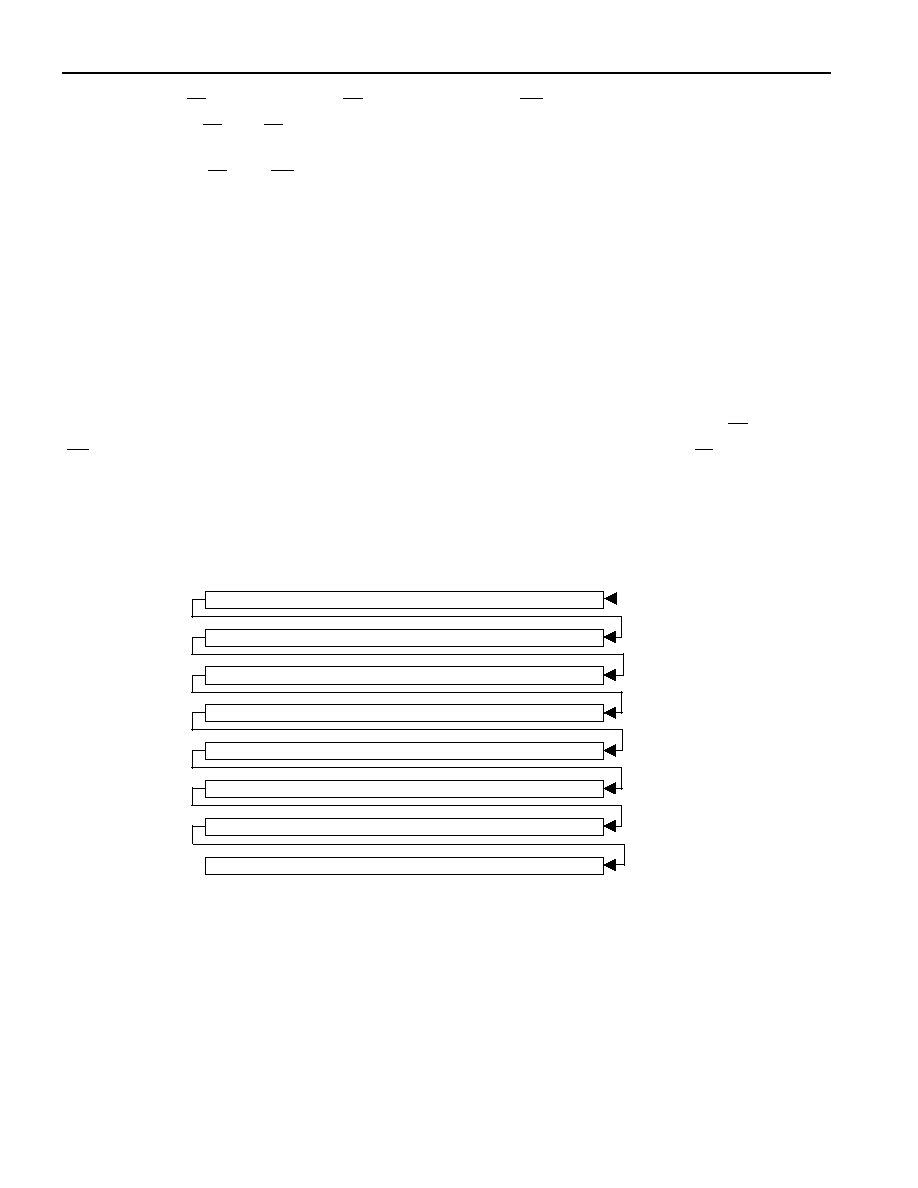
SMARTWATCH COMPARISON REGISTER DEFINITION Figure 1
NOTE:
The pattern recognition in Hex is C5, 3A, 5C, C5, 3A, A3, 5C. The odds of this pattern accidentally
duplicating and causing inadvertent entry to the SmartWatch are less than 1 in 10
19. This pattern is sent to
the SmartWatch LSB to MSB.
1
0001
0
1
0
1110
1
0
1
0
1000
1
0
1
0111
0
1
0001
0
1
0
1110
1
0
1
0
1000
1
0
1
0111
0
BYTE 0
BYTE 1
BYTE 2
BYTE 3
BYTE 4
BYTE 5
BYTE 6
BYTE 7
C5
3A
A3
5C
C5
3A
A3
5C
HEX
VALUE
7
0
相关PDF资料 |
PDF描述 |
|---|---|
| DS1216H | 0 TIMER(S), REAL TIME CLOCK, DMA32 |
| DS1216C | 0 TIMER(S), REAL TIME CLOCK, DMA28 |
| DS1216E | 0 TIMER(S), REAL TIME CLOCK, DIP28 |
| DS1225Y-200 | 8K X 8 NON-VOLATILE SRAM MODULE, 200 ns, PDIP28 |
| DS1230AB-120 | 32K X 8 NON-VOLATILE SRAM MODULE, 120 ns, DMA28 |
相关代理商/技术参数 |
参数描述 |
|---|---|
| DS1216C | 功能描述:存储器控制器 SmartWatch RAM RoHS:否 制造商:Maxim Integrated |
| DS1216D | 功能描述:存储器控制器 SmartWatch RAM RoHS:否 制造商:Maxim Integrated |
| DS1216E | 功能描述:存储器控制器 SmartWatch ROM RoHS:否 制造商:Maxim Integrated |
| DS1216F | 功能描述:IC SMART/ROM 3V 64/256/1M 32DIP RoHS:否 类别:集成电路 (IC) >> 存储器 - 控制器 系列:- 标准包装:45 系列:- 控制器类型:静态 RAM(SRAM) 电源电压:4.5 V ~ 5.5 V 工作温度:0°C ~ 70°C 封装/外壳:16-SOIC(0.295",7.50mm 宽) 供应商设备封装:16-SOIC W 包装:管件 |
| DS1216F-3 | 功能描述:IC SMART/ROM 3V 64/256/1M 32DIP RoHS:否 类别:集成电路 (IC) >> 存储器 - 控制器 系列:- 标准包装:45 系列:- 控制器类型:静态 RAM(SRAM) 电源电压:4.5 V ~ 5.5 V 工作温度:0°C ~ 70°C 封装/外壳:16-SOIC(0.295",7.50mm 宽) 供应商设备封装:16-SOIC W 包装:管件 |
发布紧急采购,3分钟左右您将得到回复。