- 您现在的位置:买卖IC网 > PDF目录299009 > DS1232LPSN-2 Voltage Detector PDF资料下载
参数资料
| 型号: | DS1232LPSN-2 |
| 英文描述: | Voltage Detector |
| 中文描述: | 电压检测器 |
| 文件页数: | 11/12页 |
| 文件大小: | 469K |
| 代理商: | DS1232LPSN-2 |
DS1230Y/AB
8 of 12
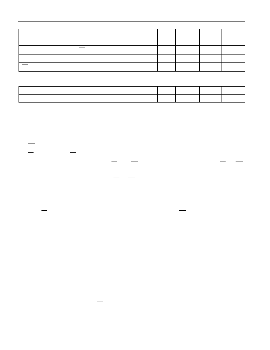
POWER-DOWN/POWER-UP TIMING
(tA: See Note 10)
PARAMETER
SYMBOL
MIN
TYP
MAX
UNITS
NOTES
CE, at VIH before Power-Down
tPD
0
s
11
VCC slew from VTP to 0V ( CE at VIH)
tF
300
s
VCC slew from 0V to VTP ( CE at VIH)
tR
300
s
CE
at VIH after Power-Up
tREC
2
125
ms
(tA=25
°C)
PARAMETER
SYMBOL
MIN
TYP
MAX
UNITS
NOTES
Expected Data Retention Time
tDR
10
years
9
WARNING:
Under no circumstance are negative undershoots, of any amplitude, allowed when device is in battery
backup mode.
NOTES:
1.
WE
is high for a Read Cycle.
2. OE = VIH or VIL. If OE = VIH during write cycle, the output buffers remain in a high-impedance state.
3. tWP is specified as the logical AND of CE and WE . tWP is measured from the latter of CE or WE
going low to the earlier of CE or WE going high.
4. tDH, tDS are measured from the earlier of CE or WE going high.
5. These parameters are sampled with a 5 pF load and are not 100% tested.
6. If the CE low transition occurs simultaneously with or latter than the WE low transition, the output
buffers remain in a high-impedance state during this period.
7. If the CE high transition occurs prior to or simultaneously with the WE high transition, the output
buffers remain in high-impedance state during this period.
8. If WE is low or the WE low transition occurs prior to or simultaneously with the CE low transition,
the output buffers remain in a high-impedance state during this period.
9. Each DS1230 has a built-in switch that disconnects the lithium source until VCC is first applied by the
user. The expected tDR is defined as accumulative time in the absence of VCC starting from the time
power is first applied by the user.
10. All AC and DC electrical characteristics are valid over the full operating temperature range. For
commercial products, this range is 0
°C to 70°C. For industrial products (IND), this range is -40°C to
+85
°C.
11. In a power-down condition the voltage on any pin may not exceed the voltage on VCC.
12. tWR1 and tDH1 are measured from WE going high.
13. tWR2 and tDH2 are measured from CE going high.
14. DS1230 DIP modules are recognized by Underwriters Laboratory (U.L.
) under file E99151.
DS1230 PowerCap modules are pending U.L. review. Contact the factory for status.
相关PDF资料 |
PDF描述 |
|---|---|
| DS1232LPU | Voltage Detector |
| DS1232LPUN | Voltage Detector |
| DS1232N | Voltage Detector |
| DS1232S | Voltage Detector |
| DS1232SN | Voltage Detector |
相关代理商/技术参数 |
参数描述 |
|---|---|
| DS1232LPSN-2/T&R | 制造商:Maxim Integrated Products 功能描述: 制造商:Maxim Integrated Products 功能描述:MICROMON. LOW POW. 8PIN SO IND. TRL - Tape and Reel 制造商:Maxim Integrated Products 功能描述:IC MICRO MONITOR LP IND 8-SOIC 制造商:Maxim Integrated Products 功能描述:Supervisory Circuits Low Power MicroMonitor Chip |
| DS1232LPSN-2/T&R | 功能描述:监控电路 Low Power MicroMonitor Chip RoHS:否 制造商:STMicroelectronics 监测电压数: 监测电压: 欠电压阈值: 过电压阈值: 输出类型:Active Low, Open Drain 人工复位:Resettable 监视器:No Watchdog 电池备用开关:No Backup 上电复位延迟(典型值):10 s 电源电压-最大:5.5 V 最大工作温度:+ 85 C 安装风格:SMD/SMT 封装 / 箱体:UDFN-6 封装:Reel |
| DS1232LPSN-2+ | 功能描述:监控电路 Low Power MicroMonitor Chip RoHS:否 制造商:STMicroelectronics 监测电压数: 监测电压: 欠电压阈值: 过电压阈值: 输出类型:Active Low, Open Drain 人工复位:Resettable 监视器:No Watchdog 电池备用开关:No Backup 上电复位延迟(典型值):10 s 电源电压-最大:5.5 V 最大工作温度:+ 85 C 安装风格:SMD/SMT 封装 / 箱体:UDFN-6 封装:Reel |
| DS1232LPSN-2+T&R | 制造商:Maxim Integrated Products 功能描述:DS1232LPSN-2+T&R Low monitor chip 制造商:Maxim Integrated Products 功能描述:PROCESSOR SUPERVISOR 4.62V 200UA 8SOIC - Tape and Reel 制造商:Maxim Integrated Products 功能描述:IC MICRO MONITOR LP IND 8-SOIC 制造商:Maxim Integrated Products 功能描述:Supervisory Circuits Low Power MicroMonitor Chip |
| DS1232LPSN-2+T&R | 功能描述:监控电路 Low Power MicroMonitor Chip RoHS:否 制造商:STMicroelectronics 监测电压数: 监测电压: 欠电压阈值: 过电压阈值: 输出类型:Active Low, Open Drain 人工复位:Resettable 监视器:No Watchdog 电池备用开关:No Backup 上电复位延迟(典型值):10 s 电源电压-最大:5.5 V 最大工作温度:+ 85 C 安装风格:SMD/SMT 封装 / 箱体:UDFN-6 封装:Reel |
发布紧急采购,3分钟左右您将得到回复。