- 您现在的位置:买卖IC网 > PDF目录378586 > DS1244Y Low-Power, 24-Bit ANALOG-TO-DIGITAL CONVERTER PDF资料下载
参数资料
| 型号: | DS1244Y |
| 英文描述: | Low-Power, 24-Bit ANALOG-TO-DIGITAL CONVERTER |
| 中文描述: | 低功耗,24位模拟数字转换器 |
| 文件页数: | 2/19页 |
| 文件大小: | 292K |
| 代理商: | DS1244Y |
ADS1244
SBAS273
2
www.ti.com
ELECTROSTATIC
DISCHARGE SENSITIVITY
This integrated circuit can be damaged by ESD. Texas Instru-
ments recommends that all integrated circuits be handled with
appropriate precautions. Failure to observe proper handling
and installation procedures can cause damage.
ESD damage can range from subtle performance degrada-
tion to complete device failure. Precision integrated circuits
may be more susceptible to damage because very small
parametric changes could cause the device not to meet its
published specifications.
ABSOLUTE MAXIMUM RATINGS
(1)
AVDD
to GND .......................................................................
–
0.3V to +6V
DVDD to GND ...................................................................
–
0.3V to +3.6V
Input Current...............................................................100mA, Momentary
Input Current................................................................ 10mA, Continuous
Analog Input Voltage to GND ..............................
–
0.5V to AVDD + 0.5V
Digital Input Voltage to GND ...............................
–
0.3V to DVDD + 0.3V
Digital Output Voltage to GND.............................
–
0.3V to DVDD + 0.3V
Maximum Junction Temperature ................................................... +150
°
C
Operating Temperature Range ........................................
–
40
°
C to +85
°
C
Storage Temperature Range .........................................
–
60
°
C to +150
°
C
Lead Temperature (soldering, 10s)............................................... +300
°
C
NOTE: (1) Stresses above those listed under
“
Absolute Maximum Ratings
”
may cause permanent damage to the device. Exposure to absolute maximum
conditions for extended periods may affect device reliability.
SPECIFIED
TEMPERATURE
RANGE
PACKAGE
DESIGNATOR
(1)
PACKAGE
MARKING
ORDERING
NUMBER
TRANSPORT
MEDIA, QUANTITY
PRODUCT
PACKAGE-LEAD
ADS1244
MSOP-10
"
DGS
"
–
40
°
C to +85
°
C
"
BHG
"
ADS1244IDGST
ADS1244IDGSR
Tape and Reel, 250
Tape and Reel, 2500
"
NOTE: (1) For the most current specifications and package information, refer to our web site at www.ti.com.
PACKAGE/ORDERING INFORMATION
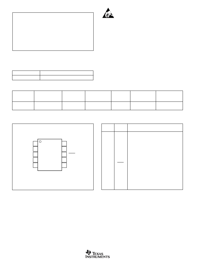
PIN CONFIGURATION
PIN
NUMBER
NAME
DESCRIPTION
1
GND
Analog and Digital Ground
2
VREFP
Positive Reference Input
3
VREFN
Negative Reference Input
4
AINN
Negative Analog Input
5
AINP
Positive Analog Input
6
AVDD
Analog Power Supply, 2.5V to 5.25V
7
DVDD
Digital Power Supply, 1.8V to 3.6V
8
DRDY/
DOUT
Dual-Purpose Output:
Data Ready: Indicates valid data by going LOW.
Data Output: Outputs data, MSB first, on the first
rising edge of SCLK.
9
SCLK
Serial Clock Input: Clocks out data on the rising
edge. Used to initiate calibration and Sleep Mode,
see text for more details.
10
CLK
System Clock Input: Typically 2.4576MHz
PIN DESCRIPTIONS
Top View
MSOP
1
2
3
4
5
10
9
8
7
6
CLK
SCLK
DRDY/DOUT
DVDD
AVDD
GND
VREFP
VREFN
AINN
AINP
ADS1244
PRODUCT
DESCRIPTION
ADS1244-EVM
ADS1244 Evaluation Module
DEMO BOARD ORDERING INFORMATION
相关PDF资料 |
PDF描述 |
|---|---|
| DS1244W-120IND | 256k NV SRAM with Phantom Clock |
| DS1244WP-120IND | 256k NV SRAM with Phantom Clock |
| DS1244YP-70 | CAT5E PATCH CORD 30 FOOT BEIGE |
| DS1244Y-70 | 256k NV SRAM with Phantom Clock |
| DS1244W-120 | 256k NV SRAM with Phantom Clock |
相关代理商/技术参数 |
参数描述 |
|---|---|
| DS1244Y120 | 制造商:Maxim Integrated Products 功能描述: |
| DS1244Y-120 | 制造商:Maxim Integrated Products 功能描述: |
| DS1244Y-150 | 制造商:Rochester Electronics LLC 功能描述: 制造商:Maxim Integrated Products 功能描述: |
| DS1244Y-200 | 制造商:DALLAS 制造商全称:Dallas Semiconductor 功能描述:256K NV SRAM with Phantom Clock |
| DS1244Y-70 | 功能描述:实时时钟 RoHS:否 制造商:Microchip Technology 功能:Clock, Calendar. Alarm RTC 总线接口:I2C 日期格式:DW:DM:M:Y 时间格式:HH:MM:SS RTC 存储容量:64 B 电源电压-最大:5.5 V 电源电压-最小:1.8 V 最大工作温度:+ 85 C 最小工作温度: 安装风格:Through Hole 封装 / 箱体:PDIP-8 封装:Tube |
发布紧急采购,3分钟左右您将得到回复。