- 您现在的位置:买卖IC网 > PDF目录9394 > DS1251Y-70+ (Maxim Integrated Products)IC NVSRAM 4MBIT 70NS 32DIP PDF资料下载
参数资料
| 型号: | DS1251Y-70+ |
| 厂商: | Maxim Integrated Products |
| 文件页数: | 14/20页 |
| 文件大小: | 0K |
| 描述: | IC NVSRAM 4MBIT 70NS 32DIP |
| 产品培训模块: | Lead (SnPb) Finish for COTS Obsolescence Mitigation Program |
| 标准包装: | 11 |
| 类型: | Phantom 计时芯片 |
| 特点: | 闰年,NVSRAM |
| 存储容量: | 512KB |
| 时间格式: | HH:MM:SS:hh(12/24 小时) |
| 数据格式: | YY-MM-DD-dd |
| 接口: | 并联 |
| 电源电压: | 4.5 V ~ 5.5 V |
| 工作温度: | 0°C ~ 70°C |
| 安装类型: | 通孔 |
| 封装/外壳: | 32-DIP 模块(0.600",15.24mm) |
| 供应商设备封装: | 32-EDIP |
| 包装: | 管件 |
DS1251/DS1251P
3 of 20
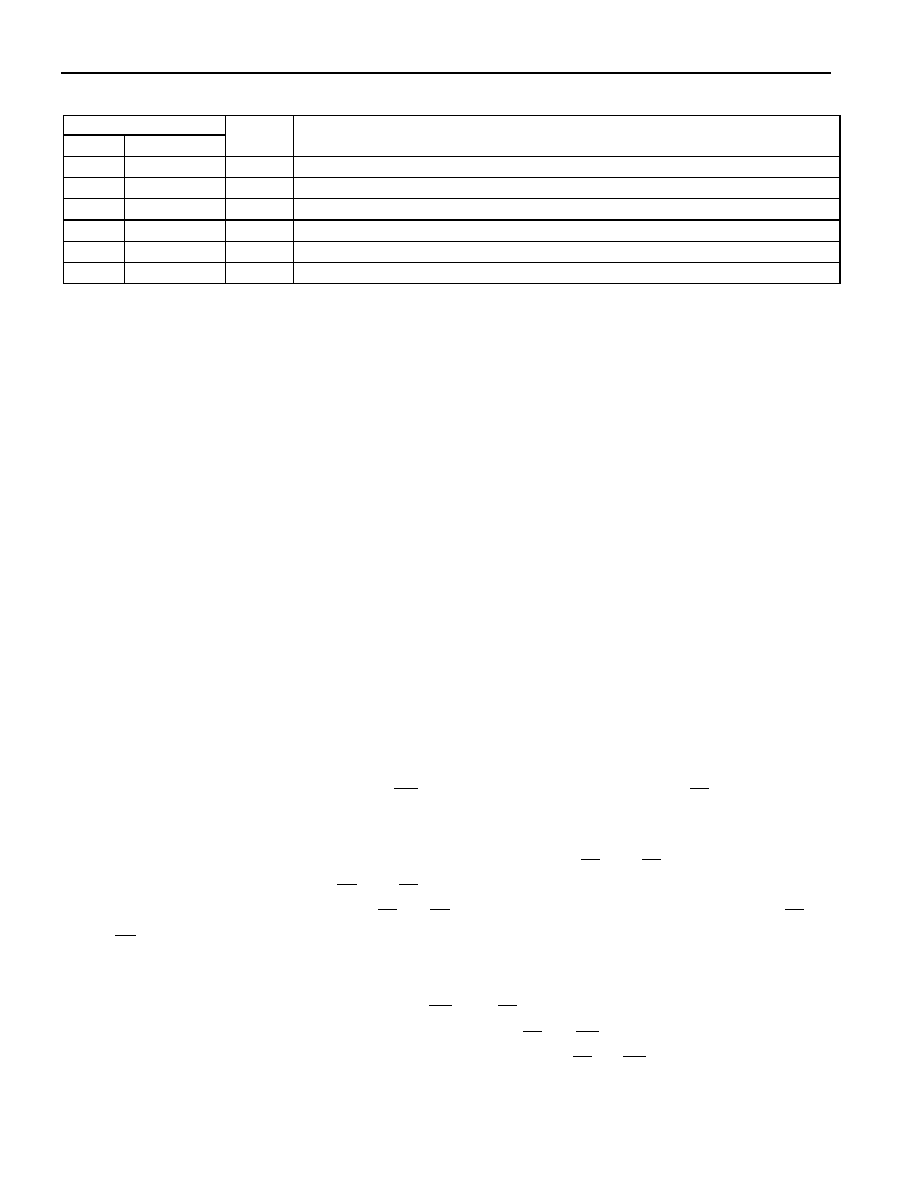
PIN DESCRIPTION (continued)
PIN
NAME
FUNCTION
EDIP
PowerCap
22
8
CE
Active-Low Chip-Enable Input
24
7
OE
Active-Low Output-Enable Input
29
6
WE
Active-Low Write-Enable Input
32
5
VCC
Power-Supply Input
—
4
N.C.
No Connection
16
17
GND
Ground
DESCRIPTION
The DS1251 4096K NV SRAM with Phantom Clock is a fully static nonvolatile RAM (organized as
512K words by 8 bits) with a built-in real-time clock. The DS1251Y has a self-contained lithium energy
source and control circuitry, which constantly monitors VCC for an out-of-tolerance condition. When such
a condition occurs, the lithium energy source is automatically switched on and write protection is
unconditionally enabled to prevent garbled data in both the memory and real-time clock.
The phantom clock provides timekeeping information including hundredths of seconds, seconds, minutes,
hours, days, dates, months, and years. The date at the end of the month is automatically adjusted for
months with fewer than 31 days, including correction for leap years. The phantom clock operates in either
24-hour or 12-hour format with an AM/PM indicator.
PACKAGES
The DS1251 is available in two packages: 32-pin DIP and 34-pin PowerCap module. The 32-pin DIP
style module integrates the crystal, lithium energy source, and silicon in one package. The 34-pin
PowerCap module board is designed with contacts for connection to a separate PowerCap (DS9034PCX)
that contains the crystal and battery. This design allows the PowerCap to be mounted on top of the
DS1251P after the completion of the surface mount process. Mounting the PowerCap after the surface
mount process prevents damage to the crystal and battery because of the high temperatures required for
solder reflow. The PowerCap is keyed to prevent reverse insertion. The PowerCap Module Board and
PowerCap are ordered separately and shipped in separate containers.
RAM READ MODE
The DS1251 executes a read cycle whenever WE (write enable) is inactive (high) and CE (chip enable) is
active (low). The unique address specified by the 19 address inputs (A0–A18) defines which of the 512K
bytes of data is to be accessed. Valid data will be available to the eight data-output drivers within tACC
(access time) after the last address input signal is stable, providing that CE and OE (output enable) access
times and states are also satisfied. If OE and CE access times are not satisfied, then data access must be
measured from the later occurring signal ( CE or OE ) and the limiting parameter is either tCO for CE or
tOE for OE , rather than address access.
RAM WRITE MODE
The DS1251 is in the write mode whenever the WE and CE signals are in the active (low) state after
address inputs are stable. The latter occurring falling edge of CE or WE will determine the start of the
write cycle. The write cycle is terminated by the earlier rising edge of CE or WE . All address inputs must
相关PDF资料 |
PDF描述 |
|---|---|
| VI-23N-MW | CONVERTER MOD DC/DC 18.5V 100W |
| VI-B2R-MY-F4 | CONVERTER MOD DC/DC 7.5V 50W |
| VI-23M-MX-B1 | CONVERTER MOD DC/DC 10V 75W |
| VI-B2R-MY-F3 | CONVERTER MOD DC/DC 7.5V 50W |
| VI-23M-MW | CONVERTER MOD DC/DC 10V 100W |
相关代理商/技术参数 |
参数描述 |
|---|---|
| DS1251Y-70+ | 功能描述:实时时钟 4096K NV SRAM w/Phantom Clock RoHS:否 制造商:Microchip Technology 功能:Clock, Calendar. Alarm RTC 总线接口:I2C 日期格式:DW:DM:M:Y 时间格式:HH:MM:SS RTC 存储容量:64 B 电源电压-最大:5.5 V 电源电压-最小:1.8 V 最大工作温度:+ 85 C 最小工作温度: 安装风格:Through Hole 封装 / 箱体:PDIP-8 封装:Tube |
| DS1251YP | 制造商:DALLAS 制造商全称:Dallas Semiconductor 功能描述:4096k NV SRAM with Phantom Clock |
| DS1251YP/WP | 制造商:MAXIM 制造商全称:Maxim Integrated Products 功能描述:PowerCap with Crystal |
| DS1251YP-100 | 制造商:Rochester Electronics LLC 功能描述: 制造商:Maxim Integrated Products 功能描述: |
| DS1251YP-70 | 功能描述:实时时钟 RoHS:否 制造商:Microchip Technology 功能:Clock, Calendar. Alarm RTC 总线接口:I2C 日期格式:DW:DM:M:Y 时间格式:HH:MM:SS RTC 存储容量:64 B 电源电压-最大:5.5 V 电源电压-最小:1.8 V 最大工作温度:+ 85 C 最小工作温度: 安装风格:Through Hole 封装 / 箱体:PDIP-8 封装:Tube |
发布紧急采购,3分钟左右您将得到回复。