- 您现在的位置:买卖IC网 > PDF目录9360 > DS12885QN+T&R (Maxim Integrated Products)IC RTC W/RAM 128 BYTE IND 28PLCC PDF资料下载
参数资料
| 型号: | DS12885QN+T&R |
| 厂商: | Maxim Integrated Products |
| 文件页数: | 8/22页 |
| 文件大小: | 0K |
| 描述: | IC RTC W/RAM 128 BYTE IND 28PLCC |
| 产品培训模块: | Lead (SnPb) Finish for COTS Obsolescence Mitigation Program |
| 标准包装: | 500 |
| 类型: | 时钟/日历 |
| 特点: | 警报器,夏令时,闰年,NVSRAM,方波输出 |
| 存储容量: | 114B |
| 时间格式: | HH:MM:SS(12/24 小时) |
| 数据格式: | YY-MM-DD-dd |
| 接口: | 并联 |
| 电源电压: | 4.5 V ~ 5.5 V |
| 电压 - 电源,电池: | 2.5 V ~ 4 V |
| 工作温度: | -40°C ~ 85°C |
| 安装类型: | 表面贴装 |
| 封装/外壳: | 28-LCC(J 形引线) |
| 供应商设备封装: | 28-PLCC(11.51x11.51) |
| 包装: | 带卷 (TR) |
DS12885/DS12887/DS12887A/DS12C887/DS12C887A
Real-Time Clocks
16
____________________________________________________________________
Bit 7: SET. When the SET bit is 0, the update transfer
functions normally by advancing the counts once per
second. When the SET bit is written to 1, any update
transfer is inhibited, and the program can initialize the
time and calendar bytes without an update occurring in
the midst of initializing. Read cycles can be executed in
a similar manner. SET is a read/write bit and is not
affected by RESET or internal functions of the device.
Bit 6: Periodic Interrupt Enable (PIE). The PIE bit is a
read/write bit that allows the periodic interrupt flag (PF) bit
in Register C to drive the IRQ pin low. When the PIE bit is
set to 1, periodic interrupts are generated by driving the
IRQ pin low at a rate specified by the RS3–RS0 bits of
Register A. A 0 in the PIE bit blocks the IRQ output from
being driven by a periodic interrupt, but the PF bit is still
set at the periodic rate. PIE is not modified by any internal
device functions, but is cleared to 0 on RESET.
Bit 5: Alarm Interrupt Enable (AIE). This bit is a
read/write bit that, when set to 1, permits the alarm flag
(AF) bit in Register C to assert IRQ. An alarm interrupt
occurs for each second that the three time bytes equal
the three alarm bytes, including a don’t-care alarm
code of binary 11XXXXXX. The AF bit does not initiate
the IRQ signal when the AIE bit is set to 0. The internal
functions of the device do not affect the AIE bit, but is
cleared to 0 on RESET.
Bit 4: Update-Ended Interrupt Enable (UIE). This bit is
a read/write bit that enables the update-end flag (UF)
bit in Register C to assert IRQ. The RESET pin going
low or the SET bit going high clears the UIE bit.
The internal functions of the device do not affect the
UIE bit, but is cleared to 0 on RESET.
Bit 3: Square-Wave Enable (SQWE). When this bit is
set to 1, a square-wave signal at the frequency set by
the rate-selection bits RS3–RS0 is driven out on the SQW
pin. When the SQWE bit is set to 0, the SQW pin is held
low. SQWE is a read/write bit and is cleared by RESET.
SQWE is low if disabled, and is high impedance when
VCC is below VPF. SQWE is cleared to 0 on RESET.
Bit 2: Data Mode (DM). This bit indicates whether time
and calendar information is in binary or BCD format.
The DM bit is set by the program to the appropriate for-
mat and can be read as required. This bit is not modi-
fied by internal functions or RESET. A 1 in DM signifies
binary data, while a 0 in DM specifies BCD data.
Bit 1: 24/12. The 24/12 control bit establishes the for-
mat of the hours byte. A 1 indicates the 24-hour mode
and a 0 indicates the 12-hour mode. This bit is
read/write and is not affected by internal functions or
RESET.
Bit 0: Daylight Saving Enable (DSE). This bit is a
read/write bit that enables two daylight saving adjust-
ments when DSE is set to 1. On the first Sunday in
April, the time increments from 1:59:59 AM to 3:00:00
AM. On the last Sunday in October when the time first
reaches 1:59:59 AM, it changes to 1:00:00 AM. When
DSE is enabled, the internal logic test for the first/last
Sunday condition at midnight. If the DSE bit is not set
when the test occurs, the daylight saving function does
not operate correctly. These adjustments do not occur
when the DSE bit is 0. This bit is not affected by internal
functions or RESET.
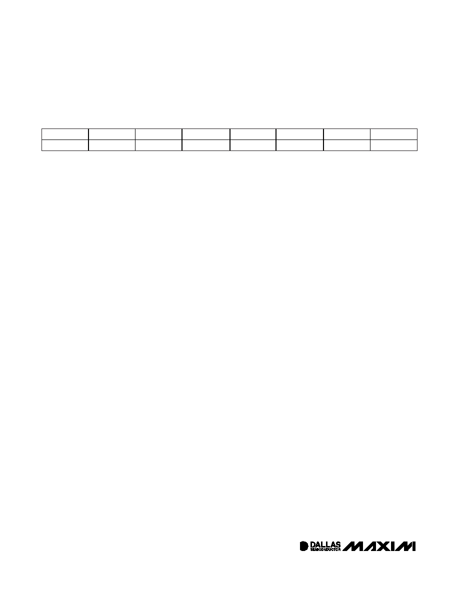
BIT 7
BIT 6
BIT 5
BIT 4
BIT 3
BIT 2
BIT 1
BIT 0
SET
PIE
AIE
UIE
SQWE
DM
24/12
DSE
Control Register B
MSB
LSB
相关PDF资料 |
PDF描述 |
|---|---|
| VI-2ND-MW | CONVERTER MOD DC/DC 85V 100W |
| VI-2NB-MX-B1 | CONVERTER MOD DC/DC 95V 75W |
| VI-2NZ-MX-F3 | CONVERTER MOD DC/DC 2V 30W |
| MAX5421BEUB+ | IC VOLTAGE DIVIDER DGLT 10MSOP |
| VI-2NB-MW | CONVERTER MOD DC/DC 95V 100W |
相关代理商/技术参数 |
参数描述 |
|---|---|
| DS12885S | 功能描述:实时时钟 RTC RoHS:否 制造商:Microchip Technology 功能:Clock, Calendar. Alarm RTC 总线接口:I2C 日期格式:DW:DM:M:Y 时间格式:HH:MM:SS RTC 存储容量:64 B 电源电压-最大:5.5 V 电源电压-最小:1.8 V 最大工作温度:+ 85 C 最小工作温度: 安装风格:Through Hole 封装 / 箱体:PDIP-8 封装:Tube |
| DS12885S/T&R | 制造商:Maxim Integrated Products 功能描述:REAL TIME CLOCK MULTIPLEXED 114BYTE 24SOIC - Tape and Reel 制造商:Maxim Integrated Products 功能描述:IC RTC W/RAM 128 BYTE 24-SOIC |
| DS12885S/T&R | 功能描述:IC RTC W/RAM 128 BYTE 24-SOIC RoHS:否 类别:集成电路 (IC) >> 时钟/计时 - 实时时钟 系列:- 产品培训模块:Obsolescence Mitigation Program 标准包装:1 系列:- 类型:时钟/日历 特点:警报器,闰年,SRAM 存储容量:- 时间格式:HH:MM:SS(12/24 小时) 数据格式:YY-MM-DD-dd 接口:SPI 电源电压:2 V ~ 5.5 V 电压 - 电源,电池:- 工作温度:-40°C ~ 85°C 安装类型:表面贴装 封装/外壳:8-WDFN 裸露焊盘 供应商设备封装:8-TDFN EP 包装:管件 |
| DS12885S+ | 功能描述:实时时钟 RTC RoHS:否 制造商:Microchip Technology 功能:Clock, Calendar. Alarm RTC 总线接口:I2C 日期格式:DW:DM:M:Y 时间格式:HH:MM:SS RTC 存储容量:64 B 电源电压-最大:5.5 V 电源电压-最小:1.8 V 最大工作温度:+ 85 C 最小工作温度: 安装风格:Through Hole 封装 / 箱体:PDIP-8 封装:Tube |
| DS12885S+T&R | 制造商:Maxim Integrated Products 功能描述:REAL TIME CLOCK MULTIPLEXED 114BYTE 24SOIC - Tape and Reel 制造商:Maxim Integrated Products 功能描述:IC RTC W/RAM 128 BYTE 24-SOIC |
发布紧急采购,3分钟左右您将得到回复。