- 您现在的位置:买卖IC网 > PDF目录9316 > DS12885T/T&R (Maxim Integrated Products)IC RTC W/RAM 128 BYTE 32-TQFP PDF资料下载
参数资料
| 型号: | DS12885T/T&R |
| 厂商: | Maxim Integrated Products |
| 文件页数: | 22/22页 |
| 文件大小: | 0K |
| 描述: | IC RTC W/RAM 128 BYTE 32-TQFP |
| 产品培训模块: | Lead (SnPb) Finish for COTS |
| 产品变化通告: | Product Discontinuation 20/Feb/2012 |
| 标准包装: | 500 |
| 类型: | 时钟/日历 |
| 特点: | 警报器,夏令时,闰年,NVSRAM,方波输出 |
| 存储容量: | 114B |
| 时间格式: | HH:MM:SS(12/24 小时) |
| 数据格式: | YY-MM-DD-dd |
| 接口: | 并联 |
| 电源电压: | 4.5 V ~ 5.5 V |
| 电压 - 电源,电池: | 2.5 V ~ 4 V |
| 工作温度: | 0°C ~ 70°C |
| 安装类型: | 表面贴装 |
| 封装/外壳: | 32-TQFP |
| 供应商设备封装: | 32-TQFP(7x7) |
| 包装: | 带卷 (TR) |
DS12885/DS12887/DS12887A/DS12C887/DS12C887A
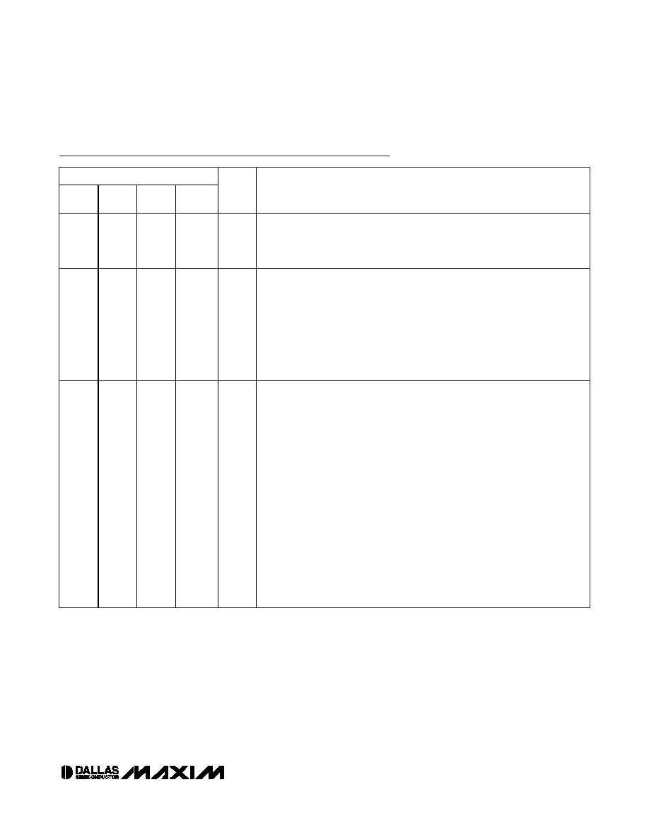
Pin Description (continued)
PIN
SO,
PDIP
EDIP
PLCC
TQFP
NAME
FUNCTION
22
2, 3,
16, 20,
21, 22
1, 11,
13, 18,
26
4, 6, 10,
15, 20,
23, 25,
27, 32
N.C.
No Connection. This pin should remain unconnected. Pin 21 is RCLR for the
DS12887A/DS12C887A. On the EDIP, these pins are missing by design.
17
21
18
DS
Data Strobe or Read Input. The DS pin has two modes of operation depending on
the level of the MOT pin. When the MOT pin is connected to VCC, Motorola bus
timing is selected. In this mode, DS is a positive pulse during the latter portion of the
bus cycle and is called data strobe. During read cycles, DS signifies the time that the
device is to drive the bidirectional bus. In write cycles, the trailing edge of DS causes
the device to latch the written data. When the MOT pin is connected to GND, Intel
bus timing is selected. DS identifies the time period when the device drives the bus
with read data. In this mode, the DS pin operates in a similar fashion as the output-
enable (OE) signal on a generic RAM.
18
22
19
RESET
Active-Low Reset Input. The RESET pin has no effect on the clock, calendar, or
RAM. On power-up, the RESET pin can be held low for a time to allow the power
supply to stabilize. The amount of time that RESET is held low is dependent on the
application. However, if RESET is used on power-up, the time RESET is low should
exceed 200ms to ensure that the internal timer that controls the device on power-
up has timed out. When RESET is low and VCC is above VPF, the following occurs:
A. Periodic interrupt-enable (PIE) bit is cleared to 0.
B. Alarm interrupt-enable (AIE) bit is cleared to 0.
C. Update-ended interrupt-enable (UIE) bit is cleared to 0.
D. Periodic-interrupt flag (PF) bit is cleared to 0.
E. Alarm-interrupt flag (AF) bit is cleared to 0.
F. Update-ended interrupt flag (UF) bit is cleared to 0.
G. Interrupt-request status flag (IRQF) bit is cleared to 0.
H. IRQ pin is in the high-impedance state.
I. The device is not accessible until RESET is returned high.
J. Square-wave output-enable (SQWE) bit is cleared to 0.
In a typical application, RESET can be connected to VCC. This connection allows
the device to go in and out of power fail without affecting any of the control
registers.
Real-Time Clocks
_____________________________________________________________________
9
相关PDF资料 |
PDF描述 |
|---|---|
| MCP4331-103E/ST | IC DGTL POT QUAD 10K 20TSSOP |
| MS3122E18-32PX | CONN RCPT 32POS BOX MNT W/PINS |
| MCP4461-502E/ST | IC POT 8BIT QUAD NONV 5K 20TSSOP |
| MCP4461T-104E/ML | IC DGTL POT 257TAPS 100K 20QFN |
| MS3122E18-32PW | CONN RCPT 32POS BOX MNT W/PINS |
相关代理商/技术参数 |
参数描述 |
|---|---|
| DS12887 | 功能描述:实时时钟 RoHS:否 制造商:Microchip Technology 功能:Clock, Calendar. Alarm RTC 总线接口:I2C 日期格式:DW:DM:M:Y 时间格式:HH:MM:SS RTC 存储容量:64 B 电源电压-最大:5.5 V 电源电压-最小:1.8 V 最大工作温度:+ 85 C 最小工作温度: 安装风格:Through Hole 封装 / 箱体:PDIP-8 封装:Tube |
| DS12887+ | 功能描述:实时时钟 RTC RoHS:否 制造商:Microchip Technology 功能:Clock, Calendar. Alarm RTC 总线接口:I2C 日期格式:DW:DM:M:Y 时间格式:HH:MM:SS RTC 存储容量:64 B 电源电压-最大:5.5 V 电源电压-最小:1.8 V 最大工作温度:+ 85 C 最小工作温度: 安装风格:Through Hole 封装 / 箱体:PDIP-8 封装:Tube |
| DS12887A | 功能描述:实时时钟 RoHS:否 制造商:Microchip Technology 功能:Clock, Calendar. Alarm RTC 总线接口:I2C 日期格式:DW:DM:M:Y 时间格式:HH:MM:SS RTC 存储容量:64 B 电源电压-最大:5.5 V 电源电压-最小:1.8 V 最大工作温度:+ 85 C 最小工作温度: 安装风格:Through Hole 封装 / 箱体:PDIP-8 封装:Tube |
| DS12887A+ | 功能描述:实时时钟 RTC RoHS:否 制造商:Microchip Technology 功能:Clock, Calendar. Alarm RTC 总线接口:I2C 日期格式:DW:DM:M:Y 时间格式:HH:MM:SS RTC 存储容量:64 B 电源电压-最大:5.5 V 电源电压-最小:1.8 V 最大工作温度:+ 85 C 最小工作温度: 安装风格:Through Hole 封装 / 箱体:PDIP-8 封装:Tube |
| DS1290 | 功能描述:计数器移位寄存器 RoHS:否 制造商:Texas Instruments 计数器类型: 计数顺序:Serial to Serial/Parallel 电路数量:1 封装 / 箱体:SOIC-20 Wide 逻辑系列: 逻辑类型: 输入线路数量:1 输出类型:Open Drain 传播延迟时间:650 ns 最大工作温度:+ 125 C 最小工作温度:- 40 C 封装:Reel |
发布紧急采购,3分钟左右您将得到回复。