- 您现在的位置:买卖IC网 > PDF目录1993 > DS1305E/T&R (Maxim Integrated Products)IC RTC SERIAL ALARM 20-TSSOP PDF资料下载
参数资料
| 型号: | DS1305E/T&R |
| 厂商: | Maxim Integrated Products |
| 文件页数: | 3/22页 |
| 文件大小: | 0K |
| 描述: | IC RTC SERIAL ALARM 20-TSSOP |
| 标准包装: | 2,500 |
| 类型: | 时钟/日历 |
| 特点: | 警报器,闰年,NVSRAM,涓流充电器 |
| 存储容量: | 96B |
| 时间格式: | HH:MM:SS(12/24 小时) |
| 数据格式: | YY-MM-DD-dd |
| 接口: | SPI |
| 电源电压: | 2 V ~ 5.5 V |
| 电压 - 电源,电池: | 2 V ~ 5.5 V |
| 工作温度: | 0°C ~ 70°C |
| 安装类型: | 表面贴装 |
| 封装/外壳: | 20-TSSOP(0.173",4.40mm 宽) |
| 供应商设备封装: | 20-TSSOP |
| 包装: | 带卷 (TR) |
DS1305
11 of 22
SERIAL INTERFACE
The DS1305 offers the flexibility to choose between two serial interface modes. The DS1305 can
communicate with the SPI interface or with a standard 3-wire interface. The interface method used is
determined by the SERMODE pin. When this pin is connected to VCC, SPI communication is selected.
When this pin is connected to ground, standard 3-wire communication is selected.
SERIAL PERIPHERAL INTERFACE (SPI)
The serial peripheral interface (SPI) is a synchronous bus for address and data transfer, and is used when
interfacing with the SPI bus on specific Motorola microcontrollers such as the 68HC05C4 and the
68HC11A8. The SPI mode of serial communication is selected by tying the SERMODE pin to VCC. Four
pins are used for the SPI. The four pins are the SDO (serial data out), SDI (serial data in), CE (chip
enable), and SCLK (serial clock). The DS1305 is the slave device in an SPI application, with the
microcontroller being the master.
The SDI and SDO pins are the serial data input and output pins for the DS1305, respectively. The CE
input is used to initiate and terminate a data transfer. The SCLK pin is used to synchronize data
movement between the master (microcontroller) and the slave (DS1305) devices.
The shift clock (SCLK), which is generated by the microcontroller, is active only during address and data
transfer to any device on the SPI bus. The inactive clock polarity is programmable in some
microcontrollers. The DS1305 determines the clock polarity by sampling SCLK when CE becomes
active. Therefore, either SCLK polarity can be accommodated. Input data (SDI) is latched on the internal
strobe edge and output data (SDO) is shifted out on the shift edge (Figure 5). There is one clock for each
bit transferred. Address and data bits are transferred in groups of eight, MSB first.
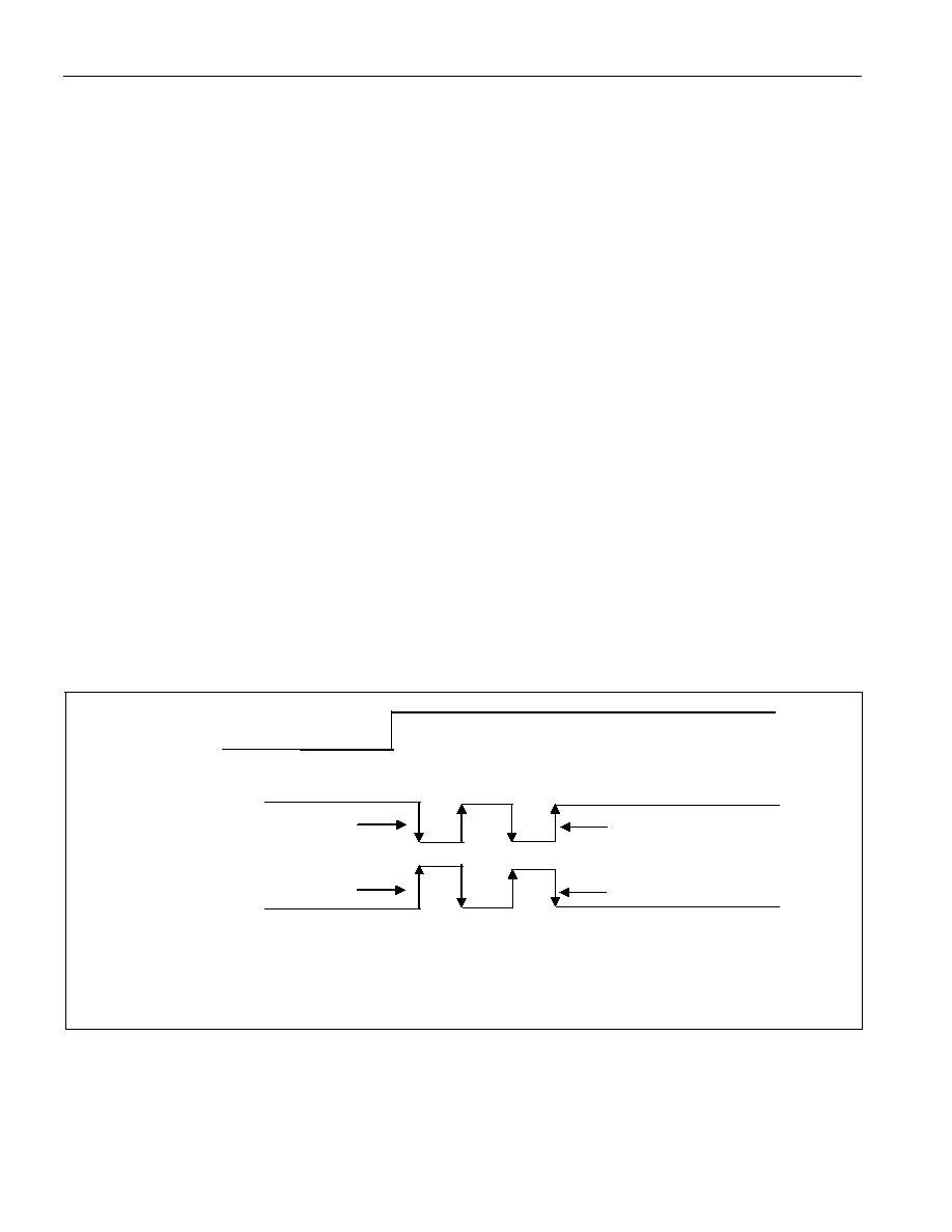
Figure 5. SERIAL CLOCK AS A FUNCTION OF MICROCONTROLLER CLOCK
POLARITY (CPOL)
CE
CPOL = 1
SCLK
DATA LATCH (WRITE)
SHIFT DATA OUT (READ)
CPOL = 0
SCLK
DATA LATCH (WRITE)
SHIFT DATA OUT (READ)
NOTE 1: CPHA BIT POLARITY (IF APPLICABLE) MAY NEED TO BE SET ACCORDINGLY.
NOTE 2: CPOL IS A BIT THAT IS SET IN THE MICROCONTROLLER’S CONTROL REGISTER.
NOTE 3: SDO REMAINS AT HIGH-Z UNTIL 8 BITS OF DATA ARE READY TO BE SHIFTED OUT DURING A READ.
相关PDF资料 |
PDF描述 |
|---|---|
| DS1306EN/T&R | IC RTC SERIAL ALARM IND 20-TSSOP |
| DS1307N | IC RTC SERIAL 512K IND 8-DIP |
| DS1308U-3+ | IC RTC 56BYTE NVRAM I2C 8UMAX |
| DS1315EN-5/T&R | IC TIME CHIP PHANTOM 20-TSSOP |
| DS1318E+ | IC COUNTER ELAPSED TIME 24-TSSOP |
相关代理商/技术参数 |
参数描述 |
|---|---|
| DS1305N | 功能描述:实时时钟 Serial Alarm RTC 3-Wire RoHS:否 制造商:Microchip Technology 功能:Clock, Calendar. Alarm RTC 总线接口:I2C 日期格式:DW:DM:M:Y 时间格式:HH:MM:SS RTC 存储容量:64 B 电源电压-最大:5.5 V 电源电压-最小:1.8 V 最大工作温度:+ 85 C 最小工作温度: 安装风格:Through Hole 封装 / 箱体:PDIP-8 封装:Tube |
| DS1305N+ | 功能描述:实时时钟 Serial Alarm RTC 3-Wire RoHS:否 制造商:Microchip Technology 功能:Clock, Calendar. Alarm RTC 总线接口:I2C 日期格式:DW:DM:M:Y 时间格式:HH:MM:SS RTC 存储容量:64 B 电源电压-最大:5.5 V 电源电压-最小:1.8 V 最大工作温度:+ 85 C 最小工作温度: 安装风格:Through Hole 封装 / 箱体:PDIP-8 封装:Tube |
| DS1305Z | 制造商:未知厂家 制造商全称:未知厂家 功能描述:Serial Alarm Real-Time Clock(287.74 k) |
| DS1306 | 功能描述:实时时钟 Serial Alarm RTC 3-Wire RoHS:否 制造商:Microchip Technology 功能:Clock, Calendar. Alarm RTC 总线接口:I2C 日期格式:DW:DM:M:Y 时间格式:HH:MM:SS RTC 存储容量:64 B 电源电压-最大:5.5 V 电源电压-最小:1.8 V 最大工作温度:+ 85 C 最小工作温度: 安装风格:Through Hole 封装 / 箱体:PDIP-8 封装:Tube |
| DS1306_05 | 制造商:DALLAS 制造商全称:Dallas Semiconductor 功能描述:Serial Alarm Real-Time Clock |
发布紧急采购,3分钟左右您将得到回复。