- 您现在的位置:买卖IC网 > PDF目录9370 > DS1340Z-3+T&R (Maxim Integrated Products)IC RTC I2C W/CHARGER 3V 8-SOIC PDF资料下载
参数资料
| 型号: | DS1340Z-3+T&R |
| 厂商: | Maxim Integrated Products |
| 文件页数: | 13/16页 |
| 文件大小: | 0K |
| 描述: | IC RTC I2C W/CHARGER 3V 8-SOIC |
| 产品培训模块: | Lead (SnPb) Finish for COTS Obsolescence Mitigation Program |
| 标准包装: | 2,500 |
| 类型: | 时钟/日历 |
| 特点: | 闰年,方波输出,涓流充电器 |
| 时间格式: | HH:MM:SS(24 小时) |
| 数据格式: | YY-MM-DD-dd |
| 接口: | I²C,2 线串口 |
| 电源电压: | 2.7 V ~ 5.5 V |
| 电压 - 电源,电池: | 1.3 V ~ 3.7 V |
| 工作温度: | -40°C ~ 85°C |
| 安装类型: | 表面贴装 |
| 封装/外壳: | 8-SOIC(0.154",3.90mm 宽) |
| 供应商设备封装: | 8-SOIC |
| 包装: | 带卷 (TR) |
I2C RTC with Trickle Charger
6
Maxim Integrated
DS1340
Detailed Description
The DS1340 is a low-power clock/calendar with a trickle
charger. Address and data are transferred serially
through a I2C bidirectional bus. The clock/calendar pro-
vides seconds, minutes, hours, day, date, month, and
year information. The date at the end of the month is
automatically adjusted for months with fewer than 31
days, including corrections for leap year. The DS1340
has a built-in power-sense circuit that detects power fail-
ures and automatically switches to the backup supply.
Power Control
The power-control function is provided by a precise,
temperature-compensated voltage reference and a
comparator circuit that monitors the VCC level. The
device is fully accessible and data can be written and
read when VCC is greater than VPF. However, when VCC
falls below VPF, the internal clock registers are blocked
from any access. If VPF is less than VBACKUP, the
device power is switched from VCC to VBACKUP when
VCC drops below VPF. If VPF is greater than VBACKUP,
the device power is switched from VCC to VBACKUP
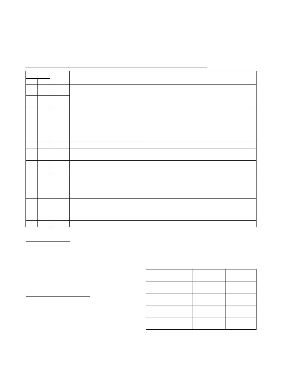
Pin Description
PIN
816
NAME
FUNCTION
1
—
X1
2
—
X2
Connections for a Standard 32.768kHz Quartz Crystal. The internal oscillator circuitry is designed for
operation with a crystal having a specified load capacitance (CL) of 12.5pF. X1 is the input to the
oscillator and can optionally be connected to an external 32.768kHz oscillator. The output of the
internal oscillator, X2, is left unconnected if an external oscillator is connected to X1.
3
14
VBACKUP
Connection for a Secondary Power Supply. For the 1.8V and 3V devices, VBACKUP must be held
between 1.3V and 3.7V for proper operation. Diodes placed in series between the supply and the input
pin may result in improper operation. VBACKUP can be as high as 5.5V on the 3.3V device.
This pin can be connected to a primary cell such as a lithium coin cell. Additionally, this pin can be
connected to a rechargeable cell or a super cap when used with the trickle-charge feature. UL
recognized to ensure against reverse charging when used with a lithium battery
(www.maximintegrated.com/qa/info/ul).
4
15
GND
Ground
5
16
SDA
Serial Data Input/Output. SDA is the data input/output for the I
2C serial interface. The SDA pin is open
drain and requires an external pullup resistor.
6
1
SCL
Serial Clock Input. SCL is the clock input for the I
2C interface and is used to synchronize data
movement on the serial interface.
7
2
FT/OUT
Frequency Test/Output. This pin is used to output either a 512Hz signal or the value of the OUT bit.
When the FT bit is logic 1, the FT/OUT pin toggles at a 512Hz rate. When the FT bit is logic 0, the
FT/OUT pin reflects the value of the OUT bit. This open-drain pin requires an external pullup resistor,
and operates with either VCC or VBACKUP applied. The pullup voltage can be up to 5.5V, regardless of
the voltage on VCC. If not used, this pin can be left unconnected.
8
3
VCC
Primary Power Supply. When voltage is applied within normal limits, the device is fully accessible and
data can be written and read. When a backup supply is connected to the device and VCC is below VPF,
reads and writes are inhibited. However, the timekeeping function continues unaffected by the lower
input voltage.
—
4–13
N.C.
No Connection. Must be connected to ground.
SUPPLY CONDITION
READ/WRITE
ACCESS
POWERED
BY
VCC < VPF,
VCC < VBACKUP
No
VBAT
VCC < VPF,
VCC > VBACKUP
No
VCC
VCC > VPF,
VCC < VBACKUP
Yes
VCC
VCC > VPF,
VCC > VBACKUP
Yes
VCC
Table 1. Power Control
相关PDF资料 |
PDF描述 |
|---|---|
| VI-J6J-MZ | CONVERTER MOD DC/DC 36V 25W |
| VE-263-MX-B1 | CONVERTER MOD DC/DC 24V 75W |
| VE-24Y-MV-B1 | CONVERTER MOD DC/DC 3.3V 99W |
| VE-24Y-MU | CONVERTER MOD DC/DC 3.3V 132W |
| VE-24X-MX-B1 | CONVERTER MOD DC/DC 5.2V 75W |
相关代理商/技术参数 |
参数描述 |
|---|---|
| DS1341 | 制造商:MAXIM 制造商全称:Maxim Integrated Products 功能描述:Low-Current I2C RTCs for High-ESR Crystals |
| DS1341_10 | 制造商:MAXIM 制造商全称:Maxim Integrated Products 功能描述:Low-Current I2C RTCs for High-ESR Crystals |
| DS1341_12 | 制造商:MAXIM 制造商全称:Maxim Integrated Products 功能描述:Low-Current I2C RTCs for High-ESR Crystals |
| DS1341T+ | 功能描述:实时时钟 I2C RTC RoHS:否 制造商:Microchip Technology 功能:Clock, Calendar. Alarm RTC 总线接口:I2C 日期格式:DW:DM:M:Y 时间格式:HH:MM:SS RTC 存储容量:64 B 电源电压-最大:5.5 V 电源电压-最小:1.8 V 最大工作温度:+ 85 C 最小工作温度: 安装风格:Through Hole 封装 / 箱体:PDIP-8 封装:Tube |
| DS1341T+T&R | 制造商:Maxim Integrated Products 功能描述:I2C RTC 6PF TDFN PB FREE T&R - Tape and Reel 制造商:Maxim Integrated Products 功能描述:IC RTC I2C W/ALARM 8TDFN |
发布紧急采购,3分钟左右您将得到回复。