- 您现在的位置:买卖IC网 > PDF目录9407 > DS1343D-3+T&R (Maxim Integrated Products)IC RTC SPI 3.0V 14TDFN-EP PDF资料下载
参数资料
| 型号: | DS1343D-3+T&R |
| 厂商: | Maxim Integrated Products |
| 文件页数: | 8/20页 |
| 文件大小: | 0K |
| 描述: | IC RTC SPI 3.0V 14TDFN-EP |
| 产品培训模块: | Lead (SnPb) Finish for COTS Obsolescence Mitigation Program |
| 标准包装: | 1 |
| 类型: | 时钟/日历 |
| 特点: | 警报器,闰年,NVRAM,方波输出,涓流充电器 |
| 存储容量: | 96B |
| 时间格式: | HH:MM:SS(12/24 小时) |
| 数据格式: | YY-MM-DD-dd |
| 接口: | SPI |
| 电源电压: | 2.7 V ~ 5.5 V |
| 电压 - 电源,电池: | 1.3 V ~ 5.5 V |
| 工作温度: | -40°C ~ 85°C |
| 安装类型: | 表面贴装 |
| 封装/外壳: | 14-WFDFN 裸露焊盘 |
| 供应商设备封装: | 14-TDFN-EP(3x3) |
| 包装: | 标准包装 |
| 其它名称: | DS1343D-3+T&RDKR |
16
Maxim Integrated
Low-Current SPI/3-Wire RTCs
DS1343/DS1344
Serial Peripheral Interface (SPI)
The serial peripheral interface (SPI) is a synchronous
bus for address and data transfer, and is used when
interfacing with the SPI bus on specific Motorola micro-
controllers, such as the 68HC05C4 and the 68HC11A8.
The SPI mode of serial communication is selected by
connecting SERMODE to VCC. Four pins are used for the
SPI. The four pins are SDO (serial-data out), SDI (serial-
data in), CE (chip enable), and SCLK (serial clock). The
IC is the slave device in an SPI application, with the
microcontroller being the master.
SDI and SDO are the serial-data input and output pins,
respectively, for the device. The CE input is used to
initiate and terminate a data transfer. SCLK is used to
synchronize data movement between the master (micro-
controller) and the slave (IC) devices.
The input clock (SCLK), which is generated by the micro-
controller, is active only during address and data transfer
to any device on the SPI bus. The inactive clock polarity
is programmable in some microcontrollers. The device
determines the clock polarity by sampling SCLK when
CE becomes active. Therefore, either SCLK polarity can
be accommodated. Input data (SDI) is latched on the
internal strobe edge and output data (SDO) is shifted out
on the shift edge (Figure 3). There is one clock for each
bit transferred. Address and data bits are transferred in
groups of eight, MSB first.
Address and Data Bytes
Address and data bytes are shifted MSB first into the
serial-data input (SDI) and out of the serial-data output
(SDO). Any transfer requires the address of the byte to
specify a write or read to either a RTC or RAM location,
followed by one or more bytes of data. Data is trans-
ferred out of the SDO for a read operation and into the
SDI for a write operation (Figure 4 and Figure 5).
The address byte is always the first byte entered after CE
is driven high. The most significant bit (R/W) of this byte
determines if a read or write takes place. If R/W is 0, one
or more read cycles occur. If R/W is 1, one or more write
cycles occur.
Data transfers can occur 1 byte at a time or in multiple-
byte burst mode. After CE is driven high an address is
written to the device. After the address, one or more data
bytes can be written or read. For a single-byte transfer,
1 byte is read or written and then CE is driven low. For
a multiple-byte transfer, however, multiple bytes can
be read or written to the device after the address has
been written. Each read or write cycle causes the RTC
register or RAM address to automatically increment.
Incrementing continues until the device is disabled.
When the RTC address space is selected, the address
wraps to 00h after incrementing from 1Fh. When the
RAM address space is selected, the address wraps to
20h after incrementing from 7Fh.
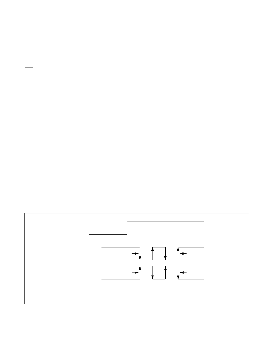
Figure 3. Serial Clock as a Function of Microcontroller Clock Polarity (CPOL)
CE
SCLK
CPOL = 1
CPOL = 0
SHIFT DATA OUT (READ)
DATA LATCH (WRITE)
SHIFT DATA OUT (READ)
NOTE 1: CPHA BIT POLARITY (IF APPLICABLE) MAY NEED TO BE SET ACCORDINGLY.
NOTE 2: CPOL IS A BIT THAT IS SET IN THE MICROCONTROLLER’S CONTROL REGISTER.
NOTE 3: SDO REMAINS AT HIGH-Z UNTIL 8 BITS OF DATA ARE READY TO BE SHIFTED OUT DURING A READ.
相关PDF资料 |
PDF描述 |
|---|---|
| VE-233-MX-B1 | CONVERTER MOD DC/DC 24V 75W |
| VE-233-MW | CONVERTER MOD DC/DC 24V 100W |
| MCP4632T-503E/MF | IC DGTL POT 50K 128TAPS 10-DFN |
| DS1344D-18+T&R | IC RTC SPI 1.8V 14TDFN-EP |
| VE-232-MX-B1 | CONVERTER MOD DC/DC 15V 75W |
相关代理商/技术参数 |
参数描述 |
|---|---|
| DS1343E-18+ | 功能描述:实时时钟 Low-Current SPI/3-Wire RTC RoHS:否 制造商:Microchip Technology 功能:Clock, Calendar. Alarm RTC 总线接口:I2C 日期格式:DW:DM:M:Y 时间格式:HH:MM:SS RTC 存储容量:64 B 电源电压-最大:5.5 V 电源电压-最小:1.8 V 最大工作温度:+ 85 C 最小工作温度: 安装风格:Through Hole 封装 / 箱体:PDIP-8 封装:Tube |
| DS1343E-18+T&R | 制造商:Maxim Integrated Products 功能描述:SPI RTC 20P TSSOP 1.8V 6PF ALRM TR - Tape and Reel 制造商:Maxim Integrated Products 功能描述:IC RTC SPI 1.8V 20TSSOP |
| DS1343E-18+T&R | 功能描述:实时时钟 Low-Current SPI/3-Wire RTC RoHS:否 制造商:Microchip Technology 功能:Clock, Calendar. Alarm RTC 总线接口:I2C 日期格式:DW:DM:M:Y 时间格式:HH:MM:SS RTC 存储容量:64 B 电源电压-最大:5.5 V 电源电压-最小:1.8 V 最大工作温度:+ 85 C 最小工作温度: 安装风格:Through Hole 封装 / 箱体:PDIP-8 封装:Tube |
| DS1343E-3+ | 功能描述:实时时钟 Low-Current SPI/3-Wire RTC RoHS:否 制造商:Microchip Technology 功能:Clock, Calendar. Alarm RTC 总线接口:I2C 日期格式:DW:DM:M:Y 时间格式:HH:MM:SS RTC 存储容量:64 B 电源电压-最大:5.5 V 电源电压-最小:1.8 V 最大工作温度:+ 85 C 最小工作温度: 安装风格:Through Hole 封装 / 箱体:PDIP-8 封装:Tube |
| DS1343E-3+T&R | 制造商:Maxim Integrated Products 功能描述:SPI RTC 20P TSSOP 3V 6PF ALRM T&R - Tape and Reel 制造商:Maxim Integrated Products 功能描述:IC RTC SPI 3.0V 20TSSOP |
发布紧急采购,3分钟左右您将得到回复。