参数资料
| 型号: | DS1343E-33+ |
| 厂商: | Maxim Integrated Products |
| 文件页数: | 3/20页 |
| 文件大小: | 0K |
| 描述: | IC RTC SPI 3.3V 20TSSOP |
| 产品培训模块: | Lead (SnPb) Finish for COTS Obsolescence Mitigation Program |
| 标准包装: | 74 |
| 类型: | 时钟/日历 |
| 特点: | 警报器,闰年,NVRAM,方波输出,涓流充电器 |
| 存储容量: | 96B |
| 时间格式: | HH:MM:SS(12/24 小时) |
| 数据格式: | YY-MM-DD-dd |
| 接口: | SPI |
| 电源电压: | 3 V ~ 5.5 V |
| 电压 - 电源,电池: | 1.3 V ~ 5.5 V |
| 工作温度: | -40°C ~ 85°C |
| 安装类型: | 表面贴装 |
| 封装/外壳: | 20-TSSOP(0.173",4.40mm 宽) |
| 供应商设备封装: | 20-TSSOP |
| 包装: | 管件 |
11
Maxim Integrated
Low-Current SPI/3-Wire RTCs
DS1343/DS1344
Register Map
Table 1 shows the devices’ register map. During a mul-
tibyte RTC access, if the address pointer reaches the
end of the register space (1Fh), it wraps around to loca-
tion 00h. During a multibyte RAM access, if the address
pointer reaches the end of the register space (7Fh), it
wraps around to location 20h. On either the rising edge
of CE or an RTC address pointer wrap around, the cur-
rent time is transferred to a secondary set of registers.
The time information is read from these secondary regis-
ters, while the clock continues to run. This eliminates the
need to reread the registers in case the main registers
update during a read.
Clock and Calendar (00h–06h)
The time and calendar information is obtained by reading
the appropriate register bytes. Table 1 shows the RTC
registers. The time and calendar are set or initialized by
writing the appropriate register bytes. The contents of
the time and calendar registers are in the BCD format.
The Day register increments at midnight and rolls over
from 7 to 1. Values that correspond to the day-of-week
are user defined, but must be sequential (i.e., if 1 equals
Sunday, then 2 equals Monday, and so on). Illogical time
and date entries result in undefined operation.
The devices can be run in either 12-hour or 24-hour
mode. Bit 6 of the Hours register is defined as the 12- or
24-hour mode-select bit. When high, the 12-hour mode
is selected. In the 12-hour mode, bit 5 is the AM/PM bit,
with a content of 1 being PM. In the 24-hour mode, bit 5
is the 20-hour field. Changing the 12/24 mode-select bit
requires that the Hours data subsequently be reentered,
including the Alarm register (if used). The Century bit (bit
7 of Month) is toggled when the Years register rolls over
from 99 to 00. On a power-on reset (POR), the time and
date are set to 00:00:00 01/01/00 (hh:mm:ss DD/MM/YY),
and the Day register is set to 01.
Alarms (07h–0Eh)
The devices contains two time-of-day/date alarms. Alarm
0 can be set by writing to registers 07h–0Ah. Alarm 1 can
be set by writing to registers 0Bh–0Eh. The alarms can
be programmed to activate the INT0 or INT1 outputs on
an alarm match condition (see Table 2). Bit 7 of each
of the time of day/date alarm registers are mask bits.
When all the mask bits for each alarm are 0, an alarm
only occurs when the values in the timekeeping registers
00h–06h match the values stored in the alarm registers.
The alarms can also be programmed to repeat every
second, minute, hour, or day. Configurations not listed
in the table result in illogical operation. POR values are
undefined.
When the RTC register values match alarm register
settings, the corresponding alarm flag bit (IRQF0 or
IRQF1) is set to 1 in the Status register. If the corre-
sponding alarm interrupt enable bit (A0IE or A1IE) is
also set to 1 in the Control register, the alarm condition
activates the output(s) defined by the INTCN bit. Upon
an active alarm, clearing the associated IRQF[1:0] bit
deasserts the selected interrupt output while leaving
the alarm enabled for the next occurrence of a match.
Alternatively, clearing the A_IE bit deasserts the output
and inhibits further output activations.
The alarm flags are always active, fully independent of
the A_IE bit states. All alarm registers should be written
to logic zero to disable the alarm matching.
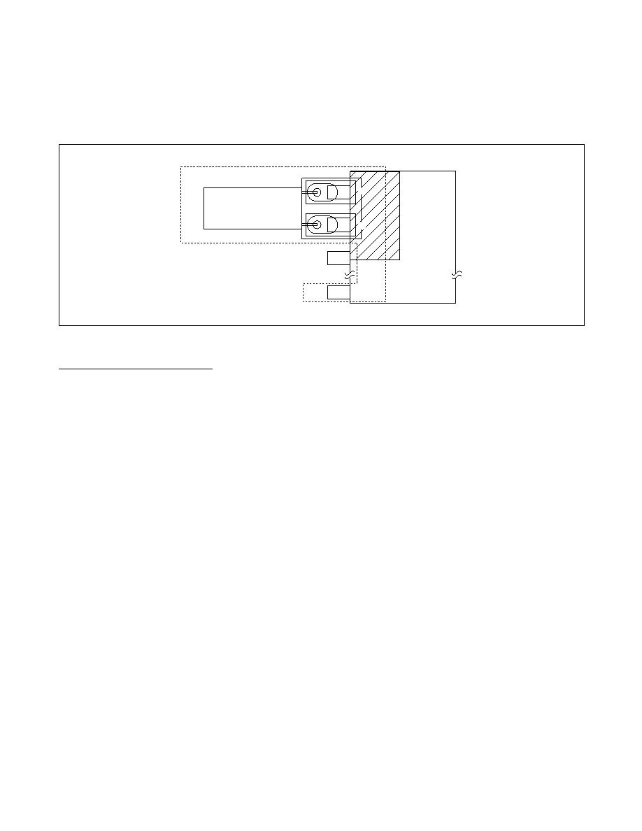
Figure 1. Layout Example
LOCAL GROUND PLANE (LAYER 2)
CRYSTAL
GND
X2
X1
NOTE: AVOID ROUTING SIGNAL LINES
IN THE CROSSHATCHED AREA
(UPPER LEFT QUADRANT) OF
THE PACKAGE UNLESS THERE IS
A GROUND PLANE BETWEEN THE
SIGNAL LINE AND THE DEVICE PACKAGE.
相关PDF资料 |
PDF描述 |
|---|---|
| VE-J0M-MZ | CONVERTER MOD DC/DC 10V 25W |
| DS1337U+ | IC RTC SERIAL 2WIRE LP 8-USOP |
| DS1337+ | IC RTC SERIAL 2WIRE LP 8-DIP |
| MAX5481ETE+ | IC 10BIT NONVOL DGTL POT 16-TQFN |
| VE-J02-MZ | CONVERTER MOD DC/DC 15V 25W |
相关代理商/技术参数 |
参数描述 |
|---|---|
| DS1343E-33+ | 功能描述:实时时钟 Low-Current SPI/3-Wire RTC RoHS:否 制造商:Microchip Technology 功能:Clock, Calendar. Alarm RTC 总线接口:I2C 日期格式:DW:DM:M:Y 时间格式:HH:MM:SS RTC 存储容量:64 B 电源电压-最大:5.5 V 电源电压-最小:1.8 V 最大工作温度:+ 85 C 最小工作温度: 安装风格:Through Hole 封装 / 箱体:PDIP-8 封装:Tube |
| DS1343E-33+T&R | 制造商:Maxim Integrated Products 功能描述:SPI RTC 20P TSSOP 3.3V 6PF ALRM T&R - Tape and Reel 制造商:Maxim Integrated Products 功能描述:IC RTC SPI 3.3V 20TSSOP |
| DS1343E-33+T&R | 功能描述:实时时钟 Low-Current SPI/3-Wire RTC RoHS:否 制造商:Microchip Technology 功能:Clock, Calendar. Alarm RTC 总线接口:I2C 日期格式:DW:DM:M:Y 时间格式:HH:MM:SS RTC 存储容量:64 B 电源电压-最大:5.5 V 电源电压-最小:1.8 V 最大工作温度:+ 85 C 最小工作温度: 安装风格:Through Hole 封装 / 箱体:PDIP-8 封装:Tube |
| DS1344 | 制造商:MAXIM 制造商全称:Maxim Integrated Products 功能描述:Low-Current SPI/3-Wire RTCs |
| DS1344D-18+ | 功能描述:实时时钟 Low-Current SPI/3-Wire RTC RoHS:否 制造商:Microchip Technology 功能:Clock, Calendar. Alarm RTC 总线接口:I2C 日期格式:DW:DM:M:Y 时间格式:HH:MM:SS RTC 存储容量:64 B 电源电压-最大:5.5 V 电源电压-最小:1.8 V 最大工作温度:+ 85 C 最小工作温度: 安装风格:Through Hole 封装 / 箱体:PDIP-8 封装:Tube |
发布紧急采购,3分钟左右您将得到回复。