- 您现在的位置:买卖IC网 > PDF目录3920 > DS1345WP-150+ (Maxim Integrated Products)IC NVSRAM 1MBIT 150NS 34PCM PDF资料下载
参数资料
| 型号: | DS1345WP-150+ |
| 厂商: | Maxim Integrated Products |
| 文件页数: | 8/10页 |
| 文件大小: | 0K |
| 描述: | IC NVSRAM 1MBIT 150NS 34PCM |
| 产品培训模块: | Lead (SnPb) Finish for COTS Obsolescence Mitigation Program |
| 标准包装: | 40 |
| 格式 - 存储器: | RAM |
| 存储器类型: | NVSRAM(非易失 SRAM) |
| 存储容量: | 1M (128K x 8) |
| 速度: | 150ns |
| 接口: | 并联 |
| 电源电压: | 3 V ~ 3.6 V |
| 工作温度: | 0°C ~ 70°C |
| 封装/外壳: | 34-PowerCap? 模块 |
| 供应商设备封装: | 34-PowerCap 模块 |
| 包装: | 管件 |
�� �
�
�DS1345W�
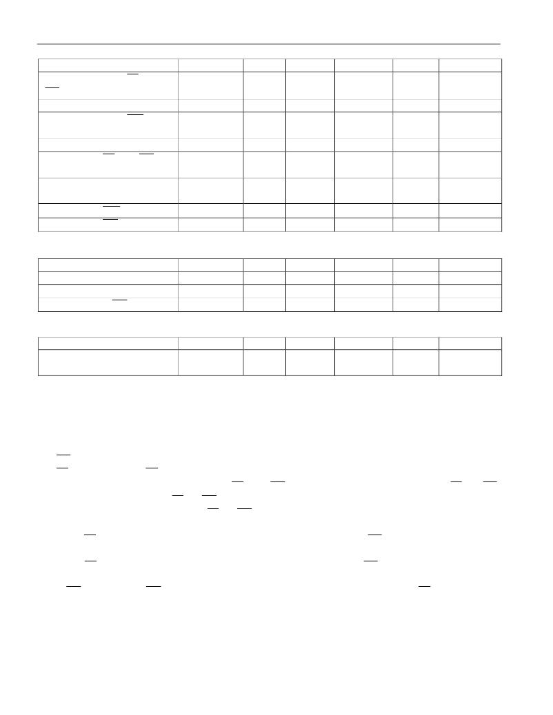
�POWER-DOWN/POWER-UP� TIMING�
�(T� A� :� See� Note� 10)�
�PARAMETER�
�V� C� C� Fail� Detect� to� CE� and�
�WE� Inactive�
�SYMBOL�
�t� PD�
�MIN�
�TYP�
�MAX�
�1.5�
�UNITS�
�μs�
�NOTES�
�11�
�V� CC� slew� from� V� TP� to� 0V�
�t� F�
�150�
�μs�
�V� CC� Fail� Detect� to� RST�
�Active�
�V� CC� slew� from� 0V� to� V� TP�
�V� CC� Valid� to� CE� and� WE�
�Inactive�
�V� CC� Valid� to� End� of� Write�
�Protection�
�t� RPD�
�t� R�
�t� PU�
�t� REC�
�150�
�15�
�2�
�125�
�μs�
�μs�
�ms�
�ms�
�14�
�V� CC� Valid� to� RST� Inactive�
�V� CC� Valid� to� BW� Valid�
�t� RPU�
�t� BPU�
�150�
�200�
�350�
�1�
�ms�
�s�
�14�
�14�
�BATTERY� WARNING� TIMING�
�(T� A� :� See� Note� 10)�
�PARAMETER�
�SYMBOL�
�MIN�
�TYP�
�MAX�
�UNITS�
�NOTES�
�Battery� Test� Cycle�
�Battery� Test� Pulse� Width�
�Battery� Test� to� BW� Active�
�t� BTC�
�t� BTPW�
�t� BW�
�24�
�1�
�1�
�hr�
�s�
�s�
�(T� A� =� +25°C)�
�PARAMETER�
�Expected� Data�
�Retention� Time�
�SYMBOL�
�t� DR�
�MIN�
�10�
�TYP�
�MAX�
�UNITS�
�years�
�NOTES�
�9�
�WARNING:�
�Under� no� circumstance� are� negative� undershoots,� of� any� amplitude,� allowed� when� device� is� in� battery�
�backup� mode.�
�NOTES:�
�1.� W� E� is� high� for� a� read� cycle.�
�2.� OE� =� V� IH� or� V� IL� .� If� OE� =� V� IH� during� write� cycle,� the� output� buffers� remain� in� a� high� impedance� state.�
�3.� t� WP� is� specified� as� the� logical� AND� of� CE� and� WE� .� t� WP� is� measured� from� the� latter� of� CE� or� WE�
�going� low� to� the� earlier� of� CE� or� WE� going� high.�
�4.� t� DS� is� measured� from� the� earlier� of� CE� or� WE� going� high.�
�5.� These� parameters� are� sampled� with� a� 5� pF� load� and� are� not� 100%� tested.�
�6.� If� the� CE� low� transition� occurs� simultaneously� with� or� latter� than� the� WE� low� transition,� the� output�
�buffers� remain� in� a� high� impedance� state� during� this� period.�
�7.� If� the� CE� high� transition� occurs� prior� to� or� simultaneously� with� the� WE� high� transition,� the� output�
�buffers� remain� in� high� impedance� state� during� this� period.�
�8.� If� WE� is� low� or� the� WE� low� transition� occurs� prior� to� or� simultaneously� with� the� CE� low� transition,�
�the� output� buffers� remain� in� a� high� impedance� state� during� this� period.�
�9.� Each� DS1345W� has� a� built-in� switch� that� disconnects� the� lithium� source� until� V� CC� is� first� applied� by�
�the� user.� The� expected� t� DR� is� defined� as� accumulative� time� in� the� absence� of� V� CC� starting� from� the�
�time� power� is� first� applied� by� the� user.�
�8� of� 10�
�相关PDF资料 |
PDF描述 |
|---|---|
| FB6S053JA1 | CONN FFC/FPC 0.3MM 53POS R/A SMD |
| AYF334965 | CONN FPC 49POS SMD Y3BW |
| DS1330WP-100+ | IC NVSRAM 256KBIT 100NS 34PCM |
| DS1330ABP-70+ | IC NVSRAM 256KBIT 70NS 34PCM |
| DS1345ABP-100+ | IC NVSRAM 1MBIT 100NS 34PCM |
相关代理商/技术参数 |
参数描述 |
|---|---|
| DS1345WP-150+ | 功能描述:NVRAM 3.3V 1024K NV SRAM w/Battery Monitor RoHS:否 制造商:Maxim Integrated 数据总线宽度:8 bit 存储容量:1024 Kbit 组织:128 K x 8 接口类型:Parallel 访问时间:70 ns 电源电压-最大:5.5 V 电源电压-最小:4.5 V 工作电流:85 mA 最大工作温度:+ 70 C 最小工作温度:0 C 封装 / 箱体:EDIP 封装:Tube |
| DS1345WP-150-IND | 制造商:DALLAS 制造商全称:Dallas Semiconductor 功能描述:3.3V 1024k Nonvolatile SRAM with Battery Monitor |
| DS1345Y | 制造商:MAXIM 制造商全称:Maxim Integrated Products 功能描述:1024k Nonvolatile SRAM with Battery Monitor |
| DS1345Y/AB | 制造商:未知厂家 制造商全称:未知厂家 功能描述:1024k Nonvolatile SRAM with Battery Monitor |
| DS1345Y-70 | 制造商:DALLAS 制造商全称:Dallas Semiconductor 功能描述:1024k Nonvolatile SRAM with Battery Monitor |
发布紧急采购,3分钟左右您将得到回复。