- 您现在的位置:买卖IC网 > PDF目录9370 > DS1390U-3+T&R (Maxim Integrated Products)IC RTC SPI 3WIRE W/CHRGR 10-MSOP PDF资料下载
参数资料
| 型号: | DS1390U-3+T&R |
| 厂商: | Maxim Integrated Products |
| 文件页数: | 16/26页 |
| 文件大小: | 0K |
| 描述: | IC RTC SPI 3WIRE W/CHRGR 10-MSOP |
| 产品培训模块: | Lead (SnPb) Finish for COTS Obsolescence Mitigation Program |
| 标准包装: | 3,000 |
| 类型: | 时钟/日历 |
| 特点: | 警报器,闰年,方波输出,涓流充电器 |
| 时间格式: | HH:MM:SS:hh(12/24 小时) |
| 数据格式: | YY-MM-DD-dd |
| 接口: | SPI |
| 电源电压: | 2.7 V ~ 3.3 V |
| 电压 - 电源,电池: | 1.3 V ~ 3.7 V |
| 工作温度: | -40°C ~ 85°C |
| 安装类型: | 表面贴装 |
| 封装/外壳: | 10-TFSOP,10-MSOP(0.118",3.00mm 宽) |
| 供应商设备封装: | 10-µMAX |
| 包装: | 带卷 (TR) |
DS1390–DS1394
Low-Voltage SPI/3-Wire RTCs with
Trickle Charger
23
Maxim Integrated
3-Wire Serial-Data Bus
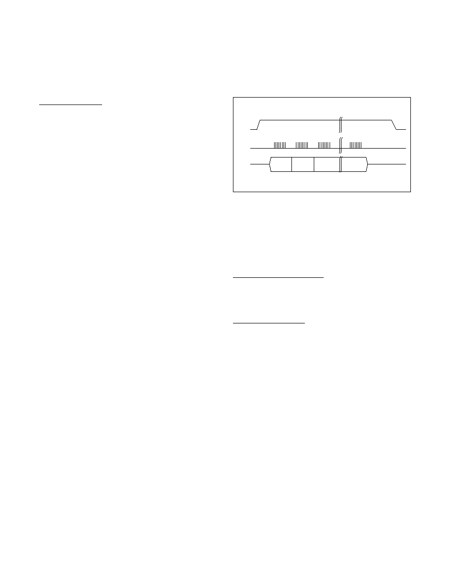
The DS1392/DS1393 provide a 3-wire serial-data bus,
and support both single-byte and multiple-byte data
transfers for maximum flexibility. The I/O pin is the seri-
al-data input/output pin. The CE input is used to initiate
and terminate a data transfer. The SCLK pin is used to
synchronize data movement between the master
(microcontroller) and the slave (DS1392/DS1393)
devices. Input data is latched on the SCLK rising edge
and output data is shifted out on the SCLK falling edge.
There is one clock for each bit transferred. Address
and data bits are transferred in groups of eight.
Address and data bytes are shifted LSB first into the
I/O pin. Data is transferred out LSB first on the I/O pin
for a read operation.
The address byte is always the first byte entered after
CE is driven high. The MSB (W/R) of this byte deter-
mines if a read or write takes place. If W/R is 0, one or
more read cycles occur. If W/R is 1, one or more write
cycles occur.
Data transfers can be one byte at a time or in multiple-
byte burst mode. After CE is driven high, an address is
written to the DS1392/DS1393. After the address, one
or more data bytes can be written or read. For a single-
byte transfer, one byte is read or written and then CE is
driven low (Figures 13 and 14). For a multiple-byte
transfer, however, multiple bytes can be read or written
after the address has been written (Figure 15). Each
read or write cycle causes the RTC register address to
automatically increment. Incrementing continues until
the device is disabled. The address wraps to 00h after
incrementing to 0Fh (during a read) and wraps to 80h
after incrementing to 8Fh (during a write). Note, howev-
er, that an updated copy of the time is only loaded into
the user-accessible copy upon the rising edge of CE.
Reading the RTC registers in a continuous loop does
not show the time advancing.
Chip Information
TRANSISTOR COUNT: 11,525
PROCESS: CMOS
SUBSTRATE CONNECTED TO GROUND
Thermal Information
Theta-JA: 180°C/W
Theta-JC: 41.9°C/W
CE
SCLK
I/O
ADDRESS
BYTE
DATA
BYTE 0
DATA
BYTE 1
DATA
BYTE N
Figure 15. 3-Wire Multiple-Byte Burst Transfer
相关PDF资料 |
PDF描述 |
|---|---|
| VI-J7Y-MZ | CONVERTER MOD DC/DC 3.3V 16.5W |
| DS1393U-18+T&R | IC RTC W/CHARGER 10-USOP |
| DS1391U-33+T&R | IC RTC W/CHARGER 10-USOP |
| VI-J6X-MZ | CONVERTER MOD DC/DC 5.2V 25W |
| DS1391U-3+T&R | IC RTC W/CHARGER 10-USOP |
相关代理商/技术参数 |
参数描述 |
|---|---|
| DS1391 | 制造商:MAXIM 制造商全称:Maxim Integrated Products 功能描述:Low-Voltage SPI/3-Wire RTCs with Trickle Charger |
| DS1391U+18 | 制造商:Maxim Integrated Products 功能描述:REAL TIME CLOCK SERL 10USOP - Bulk |
| DS1391U+3 | 制造商:Maxim Integrated Products 功能描述:REAL TIME CLOCK SERL 10USOP - Bulk |
| DS1391U+33 | 制造商:Maxim Integrated Products 功能描述:REAL TIME CLOCK SERL 10USOP - Bulk |
| DS1391U-18 | 功能描述:实时时钟 Low-V SPI/3-Wire With Trickle Charger RoHS:否 制造商:Microchip Technology 功能:Clock, Calendar. Alarm RTC 总线接口:I2C 日期格式:DW:DM:M:Y 时间格式:HH:MM:SS RTC 存储容量:64 B 电源电压-最大:5.5 V 电源电压-最小:1.8 V 最大工作温度:+ 85 C 最小工作温度: 安装风格:Through Hole 封装 / 箱体:PDIP-8 封装:Tube |
发布紧急采购,3分钟左右您将得到回复。