- 您现在的位置:买卖IC网 > PDF目录1913 > DS1482S+ (Maxim Integrated Products)IC LEVEL SHIFT 1-WIRE 16-SOIC PDF资料下载
参数资料
| 型号: | DS1482S+ |
| 厂商: | Maxim Integrated Products |
| 文件页数: | 7/7页 |
| 文件大小: | 0K |
| 描述: | IC LEVEL SHIFT 1-WIRE 16-SOIC |
| 产品培训模块: | Lead (SnPb) Finish for COTS Obsolescence Mitigation Program |
| 标准包装: | 50 |
| 类型: | 线路驱动器,发射器 |
| 驱动器/接收器数: | 1/1 |
| 电源电压: | 4.5 V ~ 5.5 V |
| 安装类型: | 表面贴装 |
| 封装/外壳: | 16-SOIC(0.295",7.50mm 宽) |
| 供应商设备封装: | 16-SOIC W |
| 包装: | 管件 |
DS1482
7 of 7
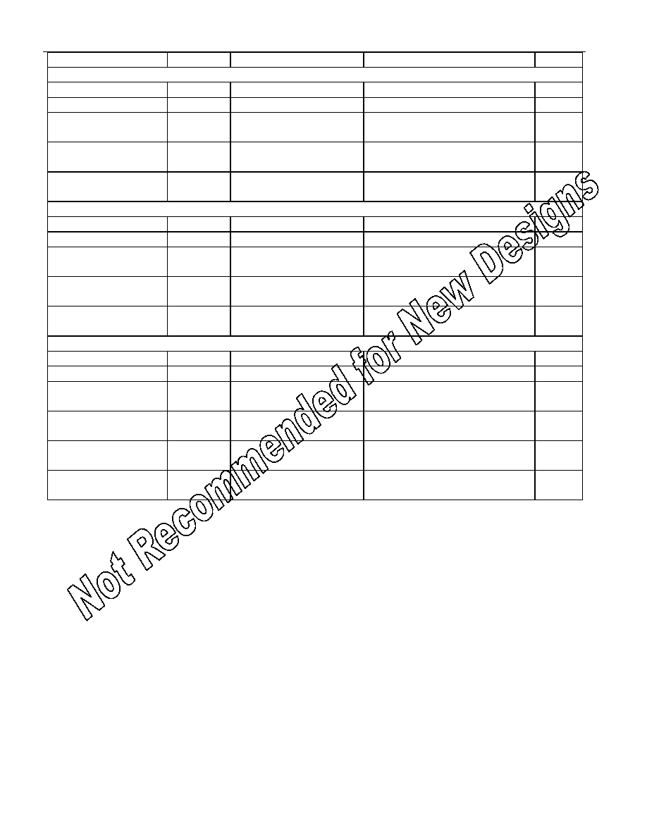
PARAMETER
SYMBOL
CONDITIONS
MIN
TYP
MAX
UNITS
OUTPUT PIN RXD
Output-Low Voltage
VOL
100A load
0.4
V
Output-High Voltage
VOH
-100A load
VCCQ - 0.5V
V
Output Rise Time
(50pF Load)
tR
0.1 x VCCQ to 0.9 x VCCQ
50
ns
Output Fall Time
(50pF Load)
tF
0.9 x VCCQ to 0.1 x VCCQ
50
ns
Delay I/O to RXD
(50pF Load)
tIR
See Figure 6 (Note 2)
100
ns
OUTPUT PIN PCTLZ
Output-Low Voltage
VOL
100A load
0.4
V
Output-High Voltage
VOH
-100A load
VCC - 0.5V
V
Output Rise Time
(50pF Load)
tR
0.1 x VCC to 0.9 x VCC
50
ns
Output Fall Time
(50pF Load)
tF
0.9 x VCC to 0.1 x VCC
50
ns
Delay SPU to PCTLZ
(50pF Load)
tSP
See Figure 7 (Note 4)
100
ns
OUTPUT PIN DONE
Output-Low Voltage
VOL
100A load
0.4
V
Output-High Voltage
VOH
-100A load
VCCQ - 0.5V
V
Output Rise Time
(50pF Load)
tR
0.1 x VCCQ to 0.9 x VCCQ
50
ns
Output Fall Time
(50pF Load)
tF
0.9 x VCCQ to 0.1 x VCCQ
50
ns
Delay I/O to DONE
(50pF Load)
tCF
START at VCCQ (Note 5)
128
500
s
Delay START to
DONE (50pF Load)
tSD
See Figure 8
100
ns
Note 1:
The input pins have a weak pulldown.
Note 2:
For OD read- or write-1 time slots, TXD should be pulsed high for 1.28s. The window for
sampling RXD begins 1.8s after TXD has turned high and ends 2.05s after TXD has turned
high. RXD must be sampled inside this window. Correct sampling can be achieved with the
particular recommended microcontroller Hitachi SH7622 if the peripheral module operating
frequency P
Φ is higher or equal to 22MHz.
Note 3:
Measured either with VCC on the pin and TXD low or with 0V on the pin and TXD high. This
parameter is guaranteed by design, and is not production tested.
Note 4:
The PCTLZ signal is gated by TXD. The PCTLZ output is only low if TXD is low.
Note 5:
Characteristic of the glitch-eating filter on the output of the load-sensing comparator, i.e., an
event where the downstream 1-Wire slave device is sinking high current, ceases sinking the
current for less than this amount of time, and resumes sinking the current does not generate
high level on DONE; DONE goes high this amount of time after the downstream 1-Wire slave
device has ceased sinking high current.
相关PDF资料 |
PDF描述 |
|---|---|
| DS14C238WM/NOPB | IC DVR/RCVR SINGLE SUPP 24-SOIC |
| DS1666-50+ | IC DIG POT 50K 14-DIP |
| DS1669-100+ | IC RHEOSTAT DALLASTAT 100K 8-DIP |
| DS1801E-014/T&R | IC POT DUAL AUDIO TAPER 14-TSSOP |
| DS1802E/T&R | IC POT DL AUDIO TAP W/PB 20TSSOP |
相关代理商/技术参数 |
参数描述 |
|---|---|
| DS1482S/R | 制造商:DALLAS 制造商全称:Dallas Semiconductor 功能描述:1-Wire Level Shifter and Line Driver with Load Sensor |
| DS1482S/T | 制造商:DALLAS 制造商全称:Dallas Semiconductor 功能描述:1-Wire Level Shifter and Line Driver with Load Sensor |
| DS1482S/T&R | 制造商:DALLAS 制造商全称:Dallas Semiconductor 功能描述:1-Wire Level Shifter and Line Driver with Load Sensor |
| DS1482S+ | 功能描述:IC LEVEL SHIFT 1-WIRE 16-SOIC RoHS:是 类别:集成电路 (IC) >> 接口 - 驱动器,接收器,收发器 系列:- 产品培训模块:Lead (SnPb) Finish for COTS Obsolescence Mitigation Program 标准包装:25 系列:- 类型:收发器 驱动器/接收器数:2/2 规程:RS232 电源电压:4.5 V ~ 5.5 V 安装类型:通孔 封装/外壳:16-DIP(0.300",7.62mm) 供应商设备封装:16-PDIP 包装:管件 |
| DS1482S+T&R | 功能描述:接口 - 专用 RoHS:否 制造商:Texas Instruments 产品类型:1080p60 Image Sensor Receiver 工作电源电压:1.8 V 电源电流:89 mA 最大功率耗散: 最大工作温度:+ 85 C 安装风格:SMD/SMT 封装 / 箱体:BGA-59 |
发布紧急采购,3分钟左右您将得到回复。