- 您现在的位置:买卖IC网 > PDF目录9358 > DS1501YEN+T&R (Maxim Integrated Products)IC RTC WDOG Y2K 5V IND 28-TSOP PDF资料下载
参数资料
| 型号: | DS1501YEN+T&R |
| 厂商: | Maxim Integrated Products |
| 文件页数: | 22/22页 |
| 文件大小: | 0K |
| 描述: | IC RTC WDOG Y2K 5V IND 28-TSOP |
| 产品培训模块: | Lead (SnPb) Finish for COTS Obsolescence Mitigation Program |
| 标准包装: | 2,500 |
| 类型: | 时钟/日历 |
| 特点: | 警报器,闰年,NVSRAM,方波输出,监视计时器,Y2K |
| 存储容量: | 256B |
| 时间格式: | HH:MM:SS(24 小时) |
| 数据格式: | YY-MM-DD-dd |
| 接口: | 并联 |
| 电源电压: | 4.5 V ~ 5.5 V |
| 电压 - 电源,电池: | 2.5 V ~ 3.7 V |
| 工作温度: | -40°C ~ 85°C |
| 安装类型: | 表面贴装 |
| 封装/外壳: | 28-TSSOP(0.465",11.8mm 宽) |
| 供应商设备封装: | 28-TSOP |
| 包装: | 带卷 (TR) |
DS1501/DS1511 Y2KC Watchdog Real-Time Clocks
9 of 22
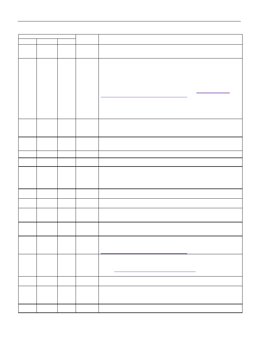
PIN DESCRIPTION
PIN
NAME
FUNCTION
SO
EDIP
TSOP
1
8
PWR
Active-Low Power-On Output (Open Drain). This output, if used, is normally
connected to power-supply control circuitry. This pin requires a pullup resistor
connected to a positive supply to operate correctly.
2, 3
—
9, 10
X1, X2
Connections for Standard 32.768kHz Quartz Crystal. For greatest accuracy, the
DS1501 must be used with a crystal that has a specified load capacitance of either
6pF or 12.5pF. The crystal select (CS) bit in control register B is used to select
operation with a 6pF or 12.5pF crystal. The crystal is attached directly to the X1 and
X2 pins. There is no need for external capacitors or resistors. An external 32.768kHz
oscillator can also drive the DS1501. In this configuration, the X1 pin is connected to
the external oscillator signal and the X2 pin is floated. For more information about
crystal selection and crystal layout considerations, refer to Application Note 58:
Crystal Considerations with Dallas Real-Time Clocks. See Figure 9. An enable bit in
the month register controls the oscillator. Oscillator startup time is highly dependent
upon crystal characteristics, PC board leakage, and layout. High ESR and excessive
capacitive loads are the major contributors to long startup times. A circuit using a
crystal with the recommended characteristics and proper layout usually starts within
one second.
4
11
RST
Active-Low Reset Output. (Open Drain). This output, if used, is normally connected
to a microprocessor-reset input. This pin requires a pull up resistor connected to a
positive supply to operate correctly. When RST is active, the device is not
accessible.
5
12
IRQ
Active-Low Interrupt Output (Open Drain). This output, if used, is normally connected
to a microprocessor interrupt input. This pin requires a pullup resistor connected to a
positive supply to operate correctly.
6–10
13–17
A4–A0
Address Inputs. Selects one of 17 register locations.
11–13,
15–19
11–13,
15–19
18–20,
22–26
DQ0–DQ7
Data Input/Output. I/O pins for 8-bit parallel data transfer.
14, 21
14
21, 28
GND
Ground. DC power is applied to the device on these pins. VCC is the positive terminal.
When power is applied within the normal limits, the device is fully accessible and
data can be written and read. When VCC drops below the normal limits, reads and
writes are inhibited. As VCC drops below the battery voltage, the RAM and
timekeeping circuits are switched over to the battery.
22
1
OE
Output-Enable Input. Active-low input that enables DQ0–DQ7 for data output from
the device.
20
27
CE
Chip-Enable Input. Active-low input to enable the device.
23
2
SQW
Square-Wave Output. When enabled, the SQW pin outputs a 32.768kHz square
wave. If the square wave (E32K) and battery backup 32kHz (BB32) bits are enabled,
power is provided by VBAUX when VCC is absent.
24
3
KS
Active-Low Kickstart Input. This pin is used to wake up a system from an external
event, such as a key closure. The KS pin is normally connected using a pullup
resistor to VBAUX. If the KS function is not used, connect to ground.
25
—
4
VBAT
Battery Input for Any Standard 3V Lithium Cell or Other Energy Source. Battery
voltage must be held between 2.5V and 3.7V for proper operation. UL recognized to
ensure against reverse charging current when used with a lithium battery.
www.maximintegrated.com/TechSupport/QA/ntrl.htm If not used, connect to ground.
26
5
VBAUX
Auxiliary Battery Input for Any Standard 3V Lithium Cell or Other Energy Source.
Battery voltage must be held between 2.5V and 3.7V for proper operation. UL
recognized to ensure against reverse charging current when used with a lithium
battery, www.maximintegrated.com/TechSupport/QA/ntrl.htm. If not used, connect to
ground.
27
6
WE
Write-Enable Input. Active-low input that enables DQ0–DQ7 for data input to the
device.
28
7
VCC
DC Power. VCC is the positive terminal. When power is applied within the normal
limits, the device is fully accessible and data can be written and read. When VCC
drops below the normal limits, reads and writes are inhibited. As VCC drops below the
battery voltage, the RAM and timekeeping circuits are switched over to the battery.
—
2, 3, 21,
25
—
N.C.
No Connect
相关PDF资料 |
PDF描述 |
|---|---|
| DS1501WEN+T&R | IC RTC WDOG Y2K 3.3V IND 28-TSOP |
| DS1678+ | IC REAL TIME EVENT REC 8-DIP |
| M83723/83R1831N | CONN RCPT 31POS WALL MT W/PINS |
| MS27484T16F42P | CONN PLUG 42POS STRAIGHT W/PINS |
| DS12885TN+ | IC RTC W/RAM 128 BYTE 32-TQFP |
相关代理商/技术参数 |
参数描述 |
|---|---|
| DS1501YN | 功能描述:IC RTC WDOG Y2KC 5V IND 28-PDIP RoHS:否 类别:集成电路 (IC) >> 时钟/计时 - 实时时钟 系列:- 产品培训模块:Obsolescence Mitigation Program 标准包装:1 系列:- 类型:时钟/日历 特点:警报器,闰年,SRAM 存储容量:- 时间格式:HH:MM:SS(12/24 小时) 数据格式:YY-MM-DD-dd 接口:SPI 电源电压:2 V ~ 5.5 V 电压 - 电源,电池:- 工作温度:-40°C ~ 85°C 安装类型:表面贴装 封装/外壳:8-WDFN 裸露焊盘 供应商设备封装:8-TDFN EP 包装:管件 |
| DS1501YN+ | 功能描述:实时时钟 Y2K-Compliant Watchdog RoHS:否 制造商:Microchip Technology 功能:Clock, Calendar. Alarm RTC 总线接口:I2C 日期格式:DW:DM:M:Y 时间格式:HH:MM:SS RTC 存储容量:64 B 电源电压-最大:5.5 V 电源电压-最小:1.8 V 最大工作温度:+ 85 C 最小工作温度: 安装风格:Through Hole 封装 / 箱体:PDIP-8 封装:Tube |
| DS1501YS | 功能描述:实时时钟 RoHS:否 制造商:Microchip Technology 功能:Clock, Calendar. Alarm RTC 总线接口:I2C 日期格式:DW:DM:M:Y 时间格式:HH:MM:SS RTC 存储容量:64 B 电源电压-最大:5.5 V 电源电压-最小:1.8 V 最大工作温度:+ 85 C 最小工作温度: 安装风格:Through Hole 封装 / 箱体:PDIP-8 封装:Tube |
| DS1501YS+ | 功能描述:实时时钟 RoHS:否 制造商:Microchip Technology 功能:Clock, Calendar. Alarm RTC 总线接口:I2C 日期格式:DW:DM:M:Y 时间格式:HH:MM:SS RTC 存储容量:64 B 电源电压-最大:5.5 V 电源电压-最小:1.8 V 最大工作温度:+ 85 C 最小工作温度: 安装风格:Through Hole 封装 / 箱体:PDIP-8 封装:Tube |
| DS1501YS+T&R | 制造商:Maxim Integrated Products 功能描述:IC RTC WDOG Y2K 5V 28-SOIC |
发布紧急采购,3分钟左右您将得到回复。