- 您现在的位置:买卖IC网 > PDF目录1994 > DS1501YSN+T&R (Maxim Integrated Products)IC RTC WDOG Y2K 5V IND 28-SOIC PDF资料下载
参数资料
| 型号: | DS1501YSN+T&R |
| 厂商: | Maxim Integrated Products |
| 文件页数: | 3/22页 |
| 文件大小: | 0K |
| 描述: | IC RTC WDOG Y2K 5V IND 28-SOIC |
| 标准包装: | 1,000 |
| 类型: | 时钟/日历 |
| 特点: | 警报器,闰年,NVSRAM,方波输出,监视计时器,Y2K |
| 存储容量: | 256B |
| 时间格式: | HH:MM:SS(24 小时) |
| 数据格式: | YY-MM-DD-dd |
| 接口: | 并联 |
| 电源电压: | 4.5 V ~ 5.5 V |
| 电压 - 电源,电池: | 2.5 V ~ 3.7 V |
| 工作温度: | -40°C ~ 85°C |
| 安装类型: | 表面贴装 |
| 封装/外壳: | 28-SOIC(0.295",7.50mm 宽) |
| 供应商设备封装: | 28-SOIC W |
| 包装: | 带卷 (TR) |
DS1501/DS1511 Y2KC Watchdog Real-Time Clocks
11 of 22
DETAILED DESCRIPTION
The DS1501/DS1511 RTC is a low-power clock/date device with a programmable day of week/date alarm. The
DS1501/DS1511 is accessed through a parallel interface. The clock/date provides seconds, minutes, hours, day,
date, month, and year information. The date at the end of the month is automatically adjusted for months with fewer
than 31 days, including corrections for leap year.
The RTC registers are double buffered into an internal and external set. The user has direct access to the external
set. Clock/calendar updates to the external set of registers can be disabled and enabled to allow the user to access
static data. When the crystal oscillator is turned on, the internal set of registers are continuously updated; this
occurs regardless of external register settings to guarantee that accurate RTC information is always maintained.
The DS1501/DS1511 contain their own power-fail circuitry that automatically deselects the device when the VCC
supply falls below a power-fail trip point. This feature provides a high degree of data security during unpredictable
system operation caused by low VCC levels.
The DS1501/DS1511 have interrupt (IRQ), power control (PWR), and reset (RST) outputs that can be used to
control CPU activity. The IRQ interrupt or RST outputs can be invoked as the result of a time-of-day alarm, CPU
watchdog alarm, or a kickstart signal. The DS1501/DS1511 power-control circuitry allow the system to be powered
on by an external stimulus, such as a keyboard or by a time and date (wakeup) alarm. The PWR output pin can be
triggered by one or either of these events, and can be used to turn on an external power supply. The PWR pin is
under software control, so that when a task is complete, the system power can then be shut down. The
DS1501/DS1511 power-on reset can be used to detect a system power-down or failure and hold the CPU in a safe
reset state until normal power returns and stabilizes; the RST output is used for this function.
The DS1501/DS1511 are clock/calendar chips with the features described above. An external crystal and battery
are the only components required to maintain time-of-day and memory status in the absence of power.
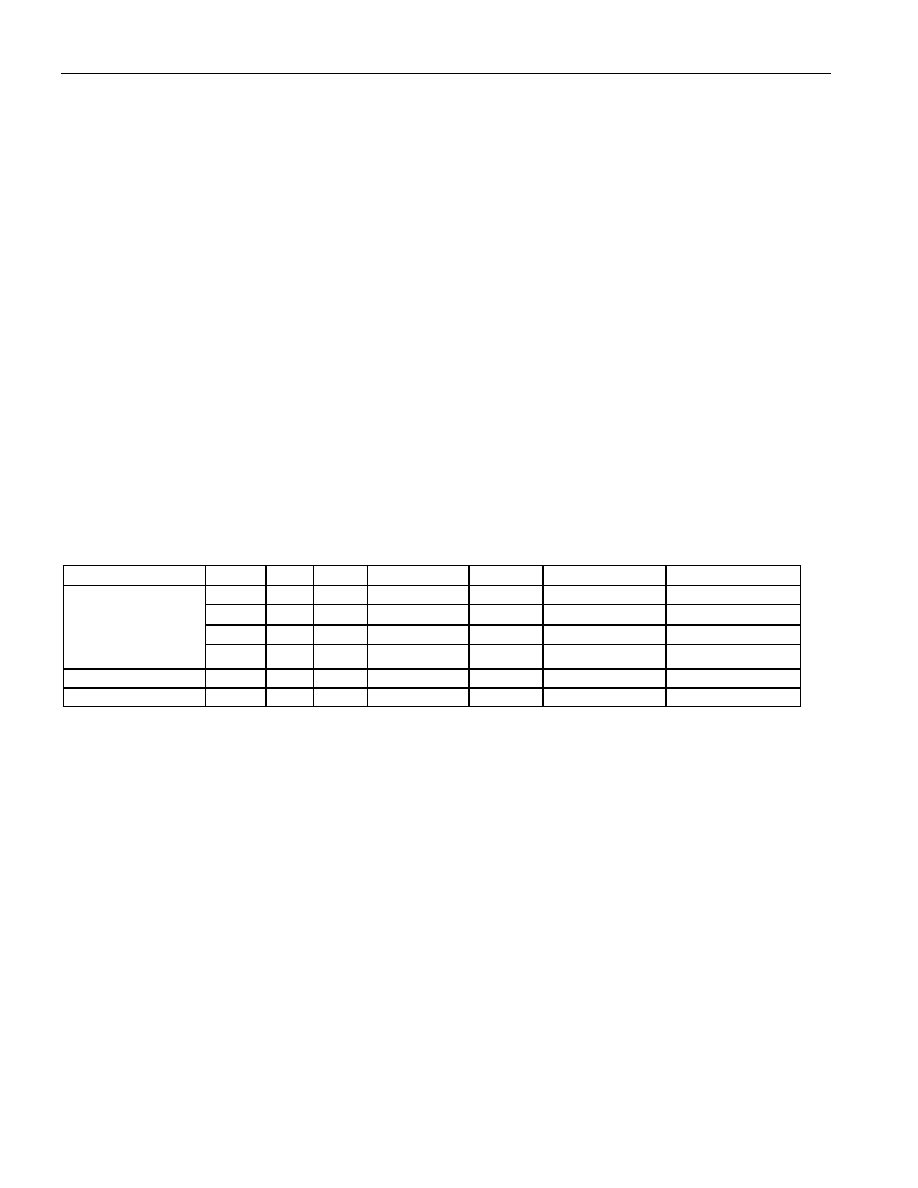
Table 1. RTC Operating Modes
VCC
CE
OE
WE
DQ0–DQ7
A0–A4
MODE
POWER
In tolerance
V
IH
X
High-Z
X
Deselect
Standby
V
IL
X
V
IL
D
IN
A
IN
Write
Active
V
IL
V
IL
V
IH
D
OUT
A
IN
Read
Active
V
IL
V
IH
V
IH
High-Z
A
IN
Read
Active
VSO < VCC < VPF
X
High-Z
X
Deselect
CMOS Standby
VCC < VSO < VPF
X
High-Z
X
Data Retention
Battery Current
DATA READ MODE
The DS1501/DS1511 are in read mode whenever CE (chip enable) and OE (output enable) are low and WE (write
enable) is high. The device architecture allows ripple-through access to any valid address location. Valid data is
available at the DQ pins within t
AA (address access) after the last address input is stable, provided that CE and OE
access times are satisfied. If CE or OE access times are not met, valid data is available at the latter of chip-enable
access (t
CSA) or at output-enable access time (tOEA). The state of the data input/output pins (DQ) is controlled by CE
and OE . If the outputs are activated before t
AA, the data lines are driven to an intermediate state until tAA. If the
address inputs are changed while CE and OE remain valid, output data remains valid for output-data hold time (t
OH)
but then goes indeterminate until the next address access (Table 1).
DATA WRITE MODE
The DS1501/DS1511 are in write mode whenever CE and WE are in their active state. The start of a write is
referenced to the latter occurring transition of CE or WE. The addresses must be held valid throughout the cycle.
CE or WE must return inactive for a minimum of t
WR prior to the initiation of a subsequent read or write cycle. Data
in must be valid t
DS prior to the end of the write and remain valid for tDH afterward. In a typical application, the OE
signal is high during a write cycle. However, OE can be active provided that care is taken with the data bus to avoid
bus contention. If OE is low prior to a high-to-low transition on WE, the data bus can become active with read data
defined by the address inputs. A low transition on WE then disables the outputs t
WEZ after WE goes active (Table
相关PDF资料 |
PDF描述 |
|---|---|
| DS1553P-70+ | IC RTC RAM Y2K 5V 70NS 34-PCM |
| DS1554W-120IND | IC RTC RAM Y2K 3.3V 120NS 32EDIP |
| DS1556WP-120IND | IC RTC RAM Y2K 3.3V 120NS 34PCM |
| DS1557P-70IND | IC RTC RAM Y2K 5V 70NS 34PCM |
| DS1558Y-TRL | IC RTC W/NV RAM 5V 48-TQFP |
相关代理商/技术参数 |
参数描述 |
|---|---|
| DS1501YZ+ | 功能描述:实时时钟 Y2K-Compliant Watchdog RoHS:否 制造商:Microchip Technology 功能:Clock, Calendar. Alarm RTC 总线接口:I2C 日期格式:DW:DM:M:Y 时间格式:HH:MM:SS RTC 存储容量:64 B 电源电压-最大:5.5 V 电源电压-最小:1.8 V 最大工作温度:+ 85 C 最小工作温度: 安装风格:Through Hole 封装 / 箱体:PDIP-8 封装:Tube |
| DS1501YZ+T&R | 制造商:Maxim Integrated Products 功能描述:Y2KC REAL TIME CLOCK 5V SOIC 300 IN - Tape and Reel 制造商:Maxim Integrated Products 功能描述:IC RTC WDOG Y2KC 5.0V 28-SOIC |
| DS1501YZ+T&R | 功能描述:实时时钟 Y2K-Compliant Watchdog RoHS:否 制造商:Microchip Technology 功能:Clock, Calendar. Alarm RTC 总线接口:I2C 日期格式:DW:DM:M:Y 时间格式:HH:MM:SS RTC 存储容量:64 B 电源电压-最大:5.5 V 电源电压-最小:1.8 V 最大工作温度:+ 85 C 最小工作温度: 安装风格:Through Hole 封装 / 箱体:PDIP-8 封装:Tube |
| DS1501YZ+TR | 制造商:MAXIM 制造商全称:Maxim Integrated Products 功能描述:Y2K-Compliant Watchdog Real-Time Clocks |
| DS1501YZN+ | 功能描述:实时时钟 Y2K-Compliant Watchdog RoHS:否 制造商:Microchip Technology 功能:Clock, Calendar. Alarm RTC 总线接口:I2C 日期格式:DW:DM:M:Y 时间格式:HH:MM:SS RTC 存储容量:64 B 电源电压-最大:5.5 V 电源电压-最小:1.8 V 最大工作温度:+ 85 C 最小工作温度: 安装风格:Through Hole 封装 / 箱体:PDIP-8 封装:Tube |
发布紧急采购,3分钟左右您将得到回复。