- 您现在的位置:买卖IC网 > PDF目录1994 > DS1683S+T&R (Maxim Integrated Products)IC REAL TIME EVENT REC 8SOIC PDF资料下载
参数资料
| 型号: | DS1683S+T&R |
| 厂商: | Maxim Integrated Products |
| 文件页数: | 9/21页 |
| 文件大小: | 0K |
| 描述: | IC REAL TIME EVENT REC 8SOIC |
| 标准包装: | 2,500 |
| 类型: | 耗用时间计数器 |
| 特点: | 警报器,EEPROM |
| 存储容量: | 16B |
| 时间格式: | 二进制 |
| 数据格式: | 二进制 |
| 接口: | I²C,2 线串口 |
| 电源电压: | 2.5 V ~ 5.5 V |
| 工作温度: | -40°C ~ 85°C |
| 安装类型: | * |
| 封装/外壳: | * |
| 供应商设备封装: | * |
| 包装: | * |
DS1683
Total-Elapsed-Time and Event Recorder with Alarm
17
Maxim Integrated
I2C Serial Interface Description
I2C Definitions
The following terminology is commonly used to
I2C AC Electrical Characteristics table for additional
information.
Master Device: The master device controls the slave
devices on the bus. The master device generates SCL
clock pulses and START and STOP conditions.
Slave Devices: Slave devices send and receive data
at the master’s request.
Bus Idle or Not Busy: Time between STOP and
START conditions when both SDA and SCL are inac-
tive and in their logic-high states. Depending on the
device, when the bus is idle it initiates a low-power
mode for slave devices.
START Condition: A START condition is generated by
the master to initiate a new data transfer with a slave.
Transitioning SDA from high to low while SCL remains
high generates a START condition.
STOP Condition: A STOP condition is generated
by the master to end a data transfer with a slave.
Transitioning SDA from low to high while SCL remains
high generates a STOP condition.
Repeated START Condition: The master can use a
repeated START condition at the end of one data trans-
fer to indicate that it will immediately initiate a new data
transfer following the current one. Repeated STARTs
are commonly used during read operations to identify
a specific memory address to begin a data transfer.
A repeated START condition is issued identically to a
normal START condition.
Bit Write: Transitions of SDA must occur during the low
state of SCL. The data on SDA must remain valid and
unchanged during the entire high pulse of SCL plus the
setup and hold time requirements. Data is shifted into
the device during the rising edge of the SCL.
Bit Read: At the end of a write operation, the master
must release the SDA bus line for the proper amount of
setup time before the next rising edge of SCL during a
bit read. The device shifts out each bit of data on SDA
at the falling edge of the previous SCL pulse and the
data bit is valid at the rising edge of the current SCL
pulse. Remember that the master generates all SCL
clock pulses including when it is reading bits from the
slave.
Acknowledgement (ACK and NACK): An acknowl-
edgement (ACK) or not-acknowledge (NACK) is
always the 9th bit transmitted during a byte transfer.
The device receiving data (the master during a read or
the slave during a write operation) performs an ACK by
transmitting a zero during the 9th bit. A device performs
a NACK by transmitting a one (done by releasing SDA)
during the 9th bit. Timing (Figure 7) for the ACK and
NACK is identical to all other bit writes. An ACK is the
acknowledgment that the device is properly receiving
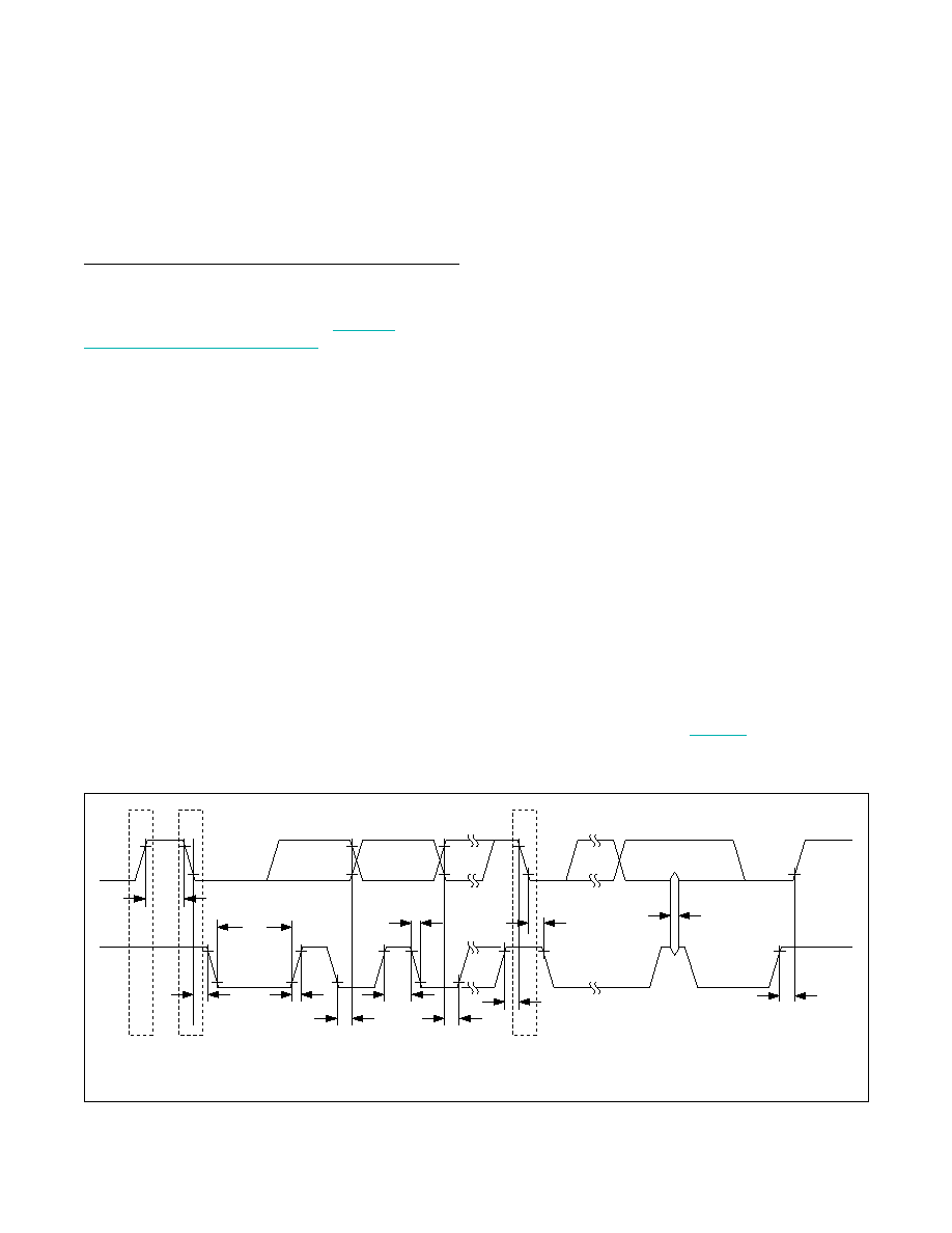
Figure 7. I2C Timing Diagram
SCL
NOTE: TIMING IS REFERENCED TO VIL(MAX) AND VIH(MIN).
SDA
STOP
START
REPEATED
START
tBUF
tHD:STA
tHD:DAT
tSU:DAT
tSU:STO
tHD:STA
tSP
tSU:STA
tHIGH
tR
tF
tLOW
相关PDF资料 |
PDF描述 |
|---|---|
| DS1685EN-5/T&R | IC RTC 5V 64BIT Y2K IND 24TSSOP |
| DS1688S+ | IC RTC W/NV RAM CTRL 28-SOIC |
| DS1689SN+T&R | IC RTC SER NV RAM CTRL IN 28SOIC |
| DS17285S-3NT | IC RTC 3V 2K NV RAM 24-SOIC |
| DS1742-100IND | IC RTC RAM Y2K 5V 100NS 24-EDIP |
相关代理商/技术参数 |
参数描述 |
|---|---|
| DS1685 | 制造商:MAXIM 制造商全称:Maxim Integrated Products 功能描述:3V/5V Real-Time Clocks |
| DS1685_05 | 制造商:DALLAS 制造商全称:Dallas Semiconductor 功能描述:3V/5V Real-Time Clocks |
| DS1685_10 | 制造商:MAXIM 制造商全称:Maxim Integrated Products 功能描述:3V/5V Real-Time Clocks |
| DS1685_12 | 制造商:MAXIM 制造商全称:Maxim Integrated Products 功能描述:3V/5V Real-Time Clocks |
| DS1685-3 | 功能描述:实时时钟 RoHS:否 制造商:Microchip Technology 功能:Clock, Calendar. Alarm RTC 总线接口:I2C 日期格式:DW:DM:M:Y 时间格式:HH:MM:SS RTC 存储容量:64 B 电源电压-最大:5.5 V 电源电压-最小:1.8 V 最大工作温度:+ 85 C 最小工作温度: 安装风格:Through Hole 封装 / 箱体:PDIP-8 封装:Tube |
发布紧急采购,3分钟左右您将得到回复。