- 您现在的位置:买卖IC网 > PDF目录295504 > DS1744WP-120+ (MAXIM INTEGRATED PRODUCTS INC) Y2K-Compliant, Nonvolatile Timekeeping RAMs PDF资料下载
参数资料
| 型号: | DS1744WP-120+ |
| 厂商: | MAXIM INTEGRATED PRODUCTS INC |
| 元件分类: | XO, clock |
| 英文描述: | Y2K-Compliant, Nonvolatile Timekeeping RAMs |
| 中文描述: | 0 TIMER(S), REAL TIME CLOCK, DMA34 |
| 封装: | ROHS COMPLIANT, MODULE-34 |
| 文件页数: | 13/16页 |
| 文件大小: | 176K |
| 代理商: | DS1744WP-120+ |
DS1744/DS1744P Y2K-Compliant, Nonvolatile Timekeeping RAMs
6 of 16
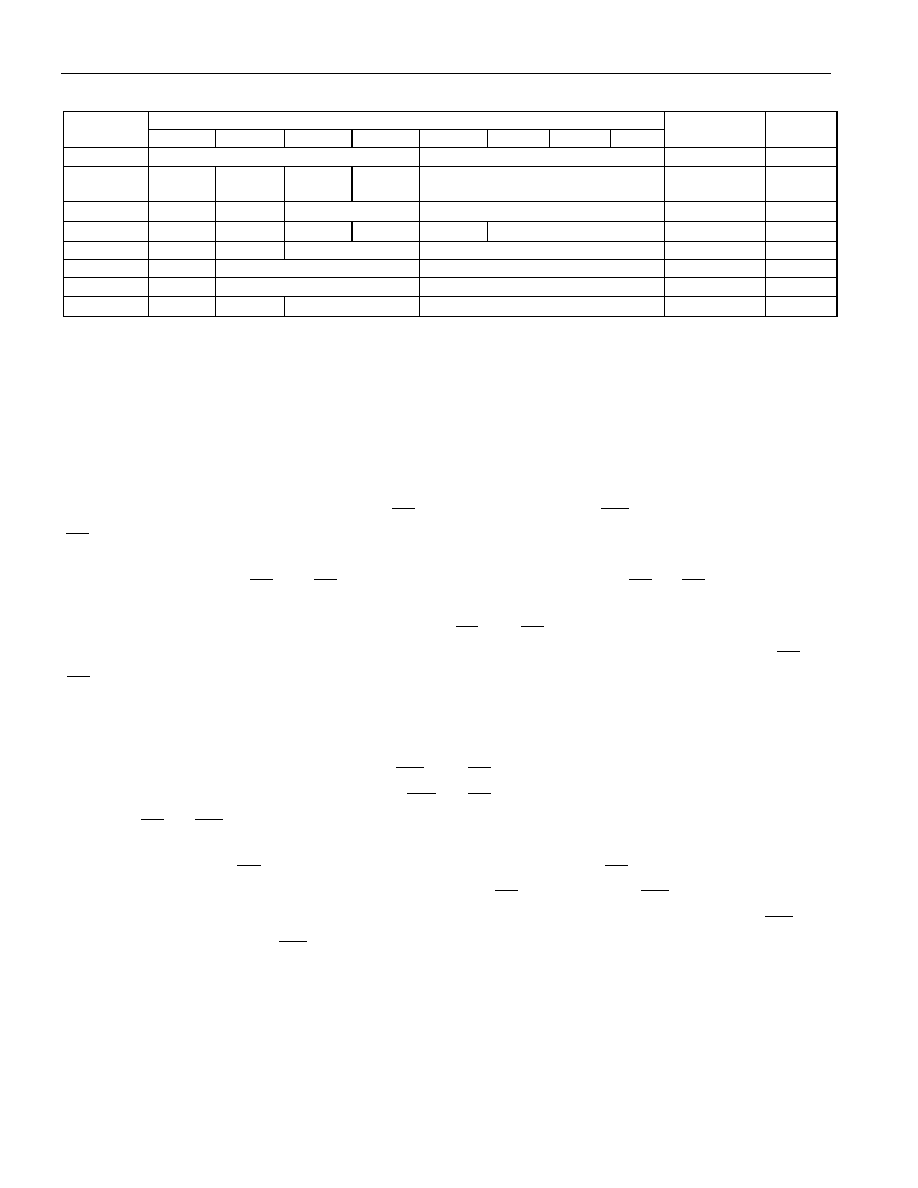
Table 2. Register Map
ADDRESS
DATA
FUNCTION
RANGE
B7
B6
B5
B4
B3
B2
B1
B0
7FFF
10 Year
Year
00-99
7FFE
X
10
Month
01-12
7FFD
X
10 Date
Date
01-31
7FFC
BF
FT
X
Day
01-07
7FFB
X
10 Hour
Hour
00-23
7FFA
X
10 Minutes
Minutes
00-59
7FF9
OSC
10 Seconds
Seconds
00-59
7FF8
W
R
10 Century
Century
00-39
OSC = Stop Bit
R = Read Bit
FT = Frequency Test
W = Write Bit
X = See Note
BF = Battery Flag
Note: All indicated “X” bits are not used but must be set to a “0” during write cycle to ensure proper
clock operation.
RETRIEVING DATA FROM RAM OR CLOCK
The DS1744 is in the read mode whenever OE (output enable) is low, WE (write enable) is high, and
CE
(chip enable) is low. The device architecture allows ripple-through access to any of the address
locations in the NV SRAM. Valid data is available at the DQ pins within tAA after the last address input is
stable, providing that the CE and OE access times and states are satisfied. If CE or OE access times and
states are not met, valid data is available at the latter of chip-enable access (tCEA) or at output-enable access
time (tOEA). The state of the DQ pins is controlled by CE and OE . If the outputs are activated before tAA,
the data lines are driven to an intermediate state until tAA. If the address inputs are changed while CE and
OE
remain valid, output data remains valid for output-data hold time (tOH) but then goes indeterminate
until the next address access.
WRITING DATA TO RAM OR CLOCK
The DS1744 is in the write mode whenever WE and CE are in their active state. The start of a write is
referenced to the latter occurring transition of WE or CE . The addresses must be held valid throughout
the cycle. CE or WE must return inactive for a minimum of tWR prior to the initiation of another read or
write cycle. Data in must be valid tDS prior to the end of write and remain valid for tDH afterward. In a
typical application, the OE signal is high during a write cycle. However, OE can be active provided that
care is taken with the data bus to avoid bus contention. If OE is low prior to WE transitioning low, the
data bus can become active with read data defined by the address inputs. A low transition on WE then
disables the output tWEZ after WE goes active.
相关PDF资料 |
PDF描述 |
|---|---|
| DS1744WP-120IND+ | Y2K-Compliant, Nonvolatile Timekeeping RAMs |
| DS1746-70+ | Y2K-Compliant, Nonvolatile Timekeeping RAMs |
| DS1746-70IND+ | Y2K-Compliant, Nonvolatile Timekeeping RAMs |
| DS1746P-70+ | Y2K-Compliant, Nonvolatile Timekeeping RAMs |
| DS1746P-70IND+ | Y2K-Compliant, Nonvolatile Timekeeping RAMs |
相关代理商/技术参数 |
参数描述 |
|---|---|
| DS1744WP-120+ | 功能描述:实时时钟 Timekeeping NV RAM RoHS:否 制造商:Microchip Technology 功能:Clock, Calendar. Alarm RTC 总线接口:I2C 日期格式:DW:DM:M:Y 时间格式:HH:MM:SS RTC 存储容量:64 B 电源电压-最大:5.5 V 电源电压-最小:1.8 V 最大工作温度:+ 85 C 最小工作温度: 安装风格:Through Hole 封装 / 箱体:PDIP-8 封装:Tube |
| DS1744WP-120IND | 功能描述:实时时钟 RoHS:否 制造商:Microchip Technology 功能:Clock, Calendar. Alarm RTC 总线接口:I2C 日期格式:DW:DM:M:Y 时间格式:HH:MM:SS RTC 存储容量:64 B 电源电压-最大:5.5 V 电源电压-最小:1.8 V 最大工作温度:+ 85 C 最小工作温度: 安装风格:Through Hole 封装 / 箱体:PDIP-8 封装:Tube |
| DS1744WP-120IND+ | 功能描述:实时时钟 Timekeeping NV RAM RoHS:否 制造商:Microchip Technology 功能:Clock, Calendar. Alarm RTC 总线接口:I2C 日期格式:DW:DM:M:Y 时间格式:HH:MM:SS RTC 存储容量:64 B 电源电压-最大:5.5 V 电源电压-最小:1.8 V 最大工作温度:+ 85 C 最小工作温度: 安装风格:Through Hole 封装 / 箱体:PDIP-8 封装:Tube |
| DS1745Y-150 | 制造商:未知厂家 制造商全称:未知厂家 功能描述:NVRAM (Battery Based) |
| DS1745Y-150-IND | 制造商:未知厂家 制造商全称:未知厂家 功能描述:NVRAM (Battery Based) |
发布紧急采购,3分钟左右您将得到回复。