- 您现在的位置:买卖IC网 > PDF目录9184 > DS1805E-010+T&R (Maxim Integrated Products)IC POT DIG ADDRESS 10K 14-TSSOP PDF资料下载
参数资料
| 型号: | DS1805E-010+T&R |
| 厂商: | Maxim Integrated Products |
| 文件页数: | 10/10页 |
| 文件大小: | 0K |
| 描述: | IC POT DIG ADDRESS 10K 14-TSSOP |
| 产品培训模块: | Lead (SnPb) Finish for COTS Obsolescence Mitigation Program |
| 标准包装: | 1,000 |
| 接片: | 256 |
| 电阻(欧姆): | 10k |
| 电路数: | 1 |
| 温度系数: | 标准值 550 ppm/°C |
| 存储器类型: | 易失 |
| 接口: | I²C(设备位址) |
| 电源电压: | 2.7 V ~ 5.5 V |
| 工作温度: | -40°C ~ 85°C |
| 安装类型: | 表面贴装 |
| 封装/外壳: | 14-TSSOP(0.173",4.40mm 宽) |
| 供应商设备封装: | 14-TSSOP |
| 包装: | 带卷 (TR) |
DS1805
Addressable Digital Potentiometer
_____________________________________________________________________
9
Following the START condition, the DS1805 monitors
the SDA bus checking the device type identifier being
transmitted. Upon receiving the 0101 address code
and appropriate device select bits, the slave device
outputs an acknowledge signal on the SDA line.
Command and Protocol
The DS1805’s command and protocol structure of the
DS1805 allows the user to read or write to both the
scratchpad and potentiometer registers. Figures 4 and
5 show the command structures for the part.
Potentiometer data values and control and command
values are always transmitted most significant bit
(MSB) first. During communications, the receiving unit
always generates the acknowledge.
Reading the DS1805
As shown in Figure 4, the DS1805 provides one read-
command operation. This operation allows the user to
read both potentiometers. Specifically, the R/W bit of the
control byte is set equal to a one for a read operation.
Communication to read the DS1805 begins with a START
condition that is issued by the master device. The control
byte from the master device follows the START condition.
Once the control byte has been received by the DS1805,
the part responds with an acknowledge. The read/write
bit of the control byte as stated should be set equal to
one for reading the DS1805.
When the master has received the acknowledge from the
DS1805, the master can then begin to receive poten-
tiometer wiper data. The value of the register-0 wiper
position will be the first returned from the DS1805. Once
the eight bits of the register-0 wiper position have been
transmitted, the master needs to issue an acknowledge,
unless it is the only byte to be read, in which case the
master issues a not acknowledge. If desired, the master
can stop the communication transfer at this point by issu-
ing the STOP condition. However, if the value of the
potentiometer-1 wiper position value is needed, commu-
nication transfer can continue by clocking the remaining
eight bits of the potentiometer-1 value, followed by a not
acknowledge. Final communication transfer is terminated
by issuing the STOP command. Figure 4 shows the flow
of the read operation.
Writing to the DS1805
Figure 5 shows a data flow diagram for writing the
DS1805. The DS1805 has three write-command opera-
tions. These include write reg-0, write pot-1, and write
reg-0/pot-1. The write reg-0 command allows the user to
write the value of scratchpad register-0 and as an option
the value of potentiometer-1. The write-1 command allows
the user to write the value of potentiometer-1 only. The
last write command, write-0/1, allows the user to write
both registers to the same value with one command and
one data value being issued.
All the write operations begin with a START condition.
Following the START condition, the master device issues
the control byte. The read/write bit of the control byte is
set to zero for writing the DS1805. Once the control byte
has been issued and the master receives the acknowl-
edgment from the DS1805, the command byte is trans-
mitted to the DS1805. As mentioned above, there exist
three write operations that can be used with the DS1805.
Figure 5 and Table 1 show the binary value of each write
command.
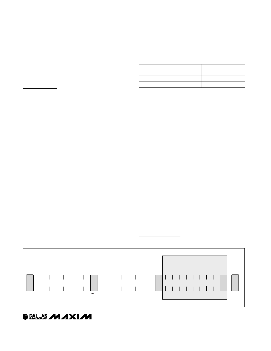
Figure 4. 2-Wire Read Protocols
MSB
ST
AR
T
ACK
NACK
STOP
CONTROL
BYTE
LSB
MSB
DATA
BYTE
LSB
MSB
OPTIONAL
DATA
BYTE
LSB
REG-0
POT-1
R/W = 1
0
1
0
1
A2
A1
A0
1
COMMAND
COMMAND VALUE
Write Register-0
101010 01
Write Potentiometer-1 Register
101010 10
Write Both Registers
101011 11
Table 1. 2-Wire Command Words
Package Information
For the latest package outline information, go to
www.maxim-ic.com/packages.
相关PDF资料 |
PDF描述 |
|---|---|
| VI-BWZ-MW-F2 | CONVERTER MOD DC/DC 2V 40W |
| VI-BWZ-MW-F1 | CONVERTER MOD DC/DC 2V 40W |
| MAX5388MAUB+ | IC DGTL POT 256POS 50K 10UMAX |
| VI-B5V-MW-B1 | CONVERTER MOD DC/DC 5.8V 100W |
| VI-BWY-MY-F4 | CONVERTER MOD DC/DC 3.3V 33W |
相关代理商/技术参数 |
参数描述 |
|---|---|
| DS1805E-050 | 制造商:MAXIM 制造商全称:Maxim Integrated Products 功能描述:Addressable Digital Potentiometer |
| DS1805E-100 | 制造商:MAXIM 制造商全称:Maxim Integrated Products 功能描述:Addressable Digital Potentiometer |
| DS1805F-010 | 制造商:Maxim Integrated Products 功能描述:SINGLE DIGITAL POTENTIOMETER - Rail/Tube |
| DS1805Z-010 | 功能描述:数字电位计 IC RoHS:否 制造商:Maxim Integrated 电阻:200 Ohms 温度系数:35 PPM / C 容差:25 % POT 数量:Dual 每 POT 分接头:256 弧刷存储器:Volatile 缓冲刷: 数字接口:Serial (3-Wire, SPI) 描述/功能:Dual Volatile Low Voltage Linear Taper Digital Potentiometer 工作电源电压:1.7 V to 5.5 V 电源电流:27 uA 最大工作温度:+ 125 C 安装风格:SMD/SMT 封装 / 箱体:TQFN-16 封装:Reel |
| DS1805Z-010+ | 功能描述:数字电位计 IC Addressable RoHS:否 制造商:Maxim Integrated 电阻:200 Ohms 温度系数:35 PPM / C 容差:25 % POT 数量:Dual 每 POT 分接头:256 弧刷存储器:Volatile 缓冲刷: 数字接口:Serial (3-Wire, SPI) 描述/功能:Dual Volatile Low Voltage Linear Taper Digital Potentiometer 工作电源电压:1.7 V to 5.5 V 电源电流:27 uA 最大工作温度:+ 125 C 安装风格:SMD/SMT 封装 / 箱体:TQFN-16 封装:Reel |
发布紧急采购,3分钟左右您将得到回复。