- 您现在的位置:买卖IC网 > PDF目录9173 > DS1805Z-010+ (Maxim Integrated Products)IC POT DIG ADDRESS 10K 16-SOIC PDF资料下载
参数资料
| 型号: | DS1805Z-010+ |
| 厂商: | Maxim Integrated Products |
| 文件页数: | 9/10页 |
| 文件大小: | 0K |
| 描述: | IC POT DIG ADDRESS 10K 16-SOIC |
| 产品培训模块: | Lead (SnPb) Finish for COTS Obsolescence Mitigation Program |
| 标准包装: | 50 |
| 接片: | 256 |
| 电阻(欧姆): | 10k |
| 电路数: | 1 |
| 温度系数: | 标准值 550 ppm/°C |
| 存储器类型: | 易失 |
| 接口: | I²C(设备位址) |
| 电源电压: | 2.7 V ~ 5.5 V |
| 工作温度: | -40°C ~ 85°C |
| 安装类型: | 表面贴装 |
| 封装/外壳: | 16-SOIC(0.154",3.90mm 宽) |
| 供应商设备封装: | 16-SOIC |
| 包装: | 管件 |
| 产品目录页面: | 1430 (CN2011-ZH PDF) |
DS1805
Addressable Digital Potentiometer
8
_____________________________________________________________________
Stop data transfer: A change in the state of the data
line from low to high while the clock line is high defines
the STOP condition.
Data valid: The state of the data line represents valid
data when, after a START condition, the data line is sta-
ble for the duration of the high period of the clock signal.
The data on the line must be changed during the low
period of the clock signal. There is one clock pulse per
bit of data. Figure 2 details how data transfer is accom-
plished on the 2-wire bus. Depending upon the state of
the R/W bit, two types of data transfer are possible.
Each data transfer is initiated with a START condition
and terminated with a STOP condition. The number of
data bytes transferred between START and STOP con-
ditions is not limited and is determined by the master
device. The information is transferred byte-wise and
each receiver acknowledges with a ninth bit.
Within the bus specifications a regular mode (100kHz
clock rate) and a fast mode (400kHz clock rate) are
defined. The DS1805 works in both modes.
Acknowledge: Each receiving device, when addressed,
is obliged to generate an acknowledge after the recep-
tion of each byte. The master device must generate an
extra clock pulse that is associated with this acknowl-
edge bit.
A device that acknowledges must pull down the SDA
line during the acknowledge clock pulse in such a way
that the SDA line is stable low during the high period of
the acknowledge-related clock pulse. Of course, setup
and hold times must be taken into account. A master
must signal an end of data to the slave by not generat-
ing an acknowledge bit on the last byte that has been
clocked out of the slave. In this case, the slave must
leave the data line high to enable the master to gener-
ate the STOP condition.
Data transfer from a master transmitter to a slave
receiver: The first byte transmitted by the master is the
control byte (slave address). Next follows a number of
data bytes. The slave returns an acknowledge bit after
each received byte.
Data transfer from a slave transmitter to a master
receiver: The first byte (the slave address) is transmit-
ted by the master. The slave then returns an acknowl-
edge bit. Next follows a number of data bytes
transmitted by the slave to the master. The master
returns an acknowledge bit after all received bytes
other than the last byte. At the end of the last received
byte, a ‘not acknowledge’ is returned.
The master device generates all of the serial clock
pulses and the START and STOP conditions. A transfer
is ended with a STOP condition or with a repeated
START condition. Since a repeated START condition is
also the beginning of the next serial transfer, the bus
will not be released.
The DS1805 can operate in the following two modes:
Slave receiver mode: Serial data and clock are
received through SDA and SCL. After each byte is
received, an acknowledge bit is transmitted. START and
STOP conditions are recognized as the beginning and
end of a serial transfer. Address recognition is performed
by hardware after reception of the slave address and
direction bit.
Slave transmitter mode: The first byte is received and
handled as in the slave receiver mode. However, in this
mode the direction bit will indicate that the transfer
direction is reversed. Serial data is transmitted on SDA
by the DS1805 while the serial clock is input on SCL.
START and STOP conditions are recognized as the
beginning and end of a serial transfer.
Slave Address
A control byte is the first byte received following the
START condition from the master device. The control
byte consists of a four-bit control code; for the DS1805,
this is set as 0101 binary for read/write operations. The
next three bits of the control byte are the device select
bits (A2, A1, A0). They are used by the master device
to select which of eight devices are to be accessed.
The select bits are the three least significant bits (LSB)
of the slave address. Additionally, A2, A1, and A0 can
be changed any time during a powered condition of the
part. The last bit of the control byte (R/W) defines the
operation to be performed. When set to a one, a read
operation is selected; when set to a zero a write opera-
tion is selected. Figure 3 shows the control byte struc-
ture for the DS1805.
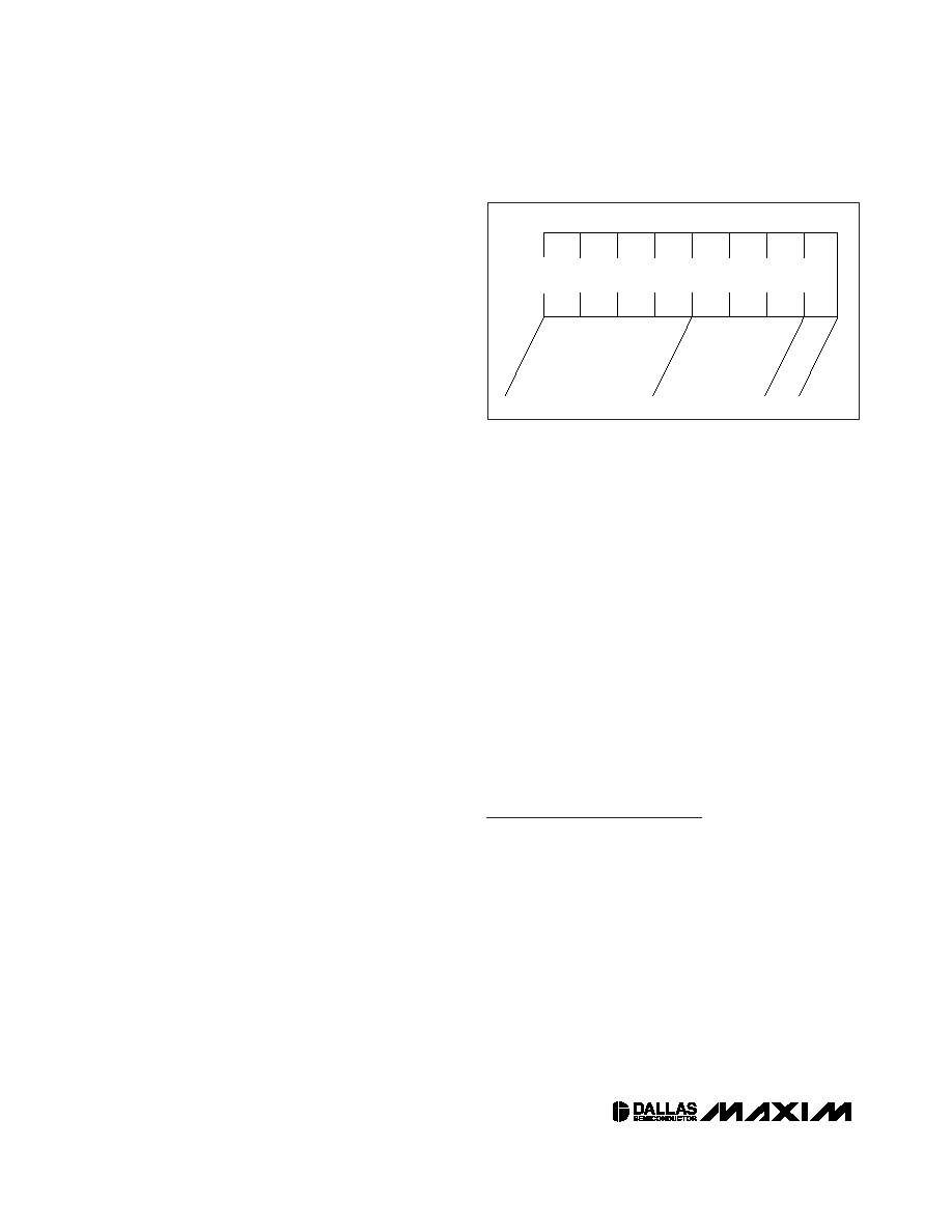
Figure 3. Control Byte
MSB
DEVICE
IDENTIFIER
DEVICE
ADDRESS
READ/WRITE
BIT
0
1
0
1
A2
A1
A0
R/W
LSB
相关PDF资料 |
PDF描述 |
|---|---|
| MS27484T22B2P | CONN PLUG 85POS STRAIGHT W/PINS |
| DS1807E+T&R | IC POT ADDRESS 2X AUDIO 14-TSSOP |
| MS27466T23F53S | CONN RCPT 53POS WALL MT W/SCKT |
| DS1801E-014+T&R | IC POT DUAL AUDIO TAPER 14-TSSOP |
| 7WBD3306AMUTCG | TRANSLATOR 2BIT FST BUS SW 8UDFN |
相关代理商/技术参数 |
参数描述 |
|---|---|
| DS1805Z-010+ | 功能描述:数字电位计 IC Addressable RoHS:否 制造商:Maxim Integrated 电阻:200 Ohms 温度系数:35 PPM / C 容差:25 % POT 数量:Dual 每 POT 分接头:256 弧刷存储器:Volatile 缓冲刷: 数字接口:Serial (3-Wire, SPI) 描述/功能:Dual Volatile Low Voltage Linear Taper Digital Potentiometer 工作电源电压:1.7 V to 5.5 V 电源电流:27 uA 最大工作温度:+ 125 C 安装风格:SMD/SMT 封装 / 箱体:TQFN-16 封装:Reel |
| DS1805Z-010+T&R | 制造商:Maxim Integrated Products 功能描述:SINGLE DIGITAL POT LEAD FREE |
| DS1805Z-050 | 制造商:MAXIM 制造商全称:Maxim Integrated Products 功能描述:Addressable Digital Potentiometer |
| DS1805Z-10 | 制造商:Maxim Integrated Products 功能描述: |
| DS1805Z-100 | 制造商:MAXIM 制造商全称:Maxim Integrated Products 功能描述:Addressable Digital Potentiometer |
发布紧急采购,3分钟左右您将得到回复。