- 您现在的位置:买卖IC网 > PDF目录2067 > DS1843D+ (Maxim Integrated Products)IC CIRCUIT SAMPLE-N-HOLD 8-UDFN PDF资料下载
参数资料
| 型号: | DS1843D+ |
| 厂商: | Maxim Integrated Products |
| 文件页数: | 7/8页 |
| 文件大小: | 0K |
| 描述: | IC CIRCUIT SAMPLE-N-HOLD 8-UDFN |
| 产品培训模块: | Lead (SnPb) Finish for COTS Obsolescence Mitigation Program |
| 标准包装: | 1 |
| 类型: | 采样和保持 |
| 应用: | 光纤学网络 |
| 安装类型: | 表面贴装 |
| 封装/外壳: | 8-WFDFN |
| 供应商设备封装: | 8-uDFN(2x2) |
| 包装: | 管件 |
DS1843
Fast Sample-and-Hold Circuit
_______________________________________________________________________________________
7
Applications Information
Power-Supply Decoupling
To achieve the best results when using the DS1843,
decouple the power-supply pin, VCC, with a 0.01F or
0.1F capacitor. Use a high-quality X7R or equivalent
ceramic surface-mount capacitor.
DS1843 Estimated Settling Time
The settling time is dependent on the gain ratio of the
current mirror used at the input of the DS1843. For
example, the MAX4007 includes a 10:1 ratio current
mirror. This requires a 5k
resistor to create a 1V full-
scale output with 2mA current input to the MAX4007.
This resistor can be decreased to 2.5k
by using the
DS1842, which has a 5:1 ratio current mirror.
Variable Definitions:
RIN: Input resistor. The current mirror creates a voltage
across this resistor.
RSW: Resistance of series switch that connects internal
circuitry to input pins after tIST time.
CIN: 7pF parasitic (ESD) capacitor.
CPAR: External parasitic capacitance. A current mirror's
output and typical trace capacitance are less than
10pF.
CS: 5pF sample capacitor.
tIST: Internal settling time based on tS from the AC elec-
trical specification. The minimum tS includes one time
constant. tIST removes this time constant.
tRC: RC settling time of the input.
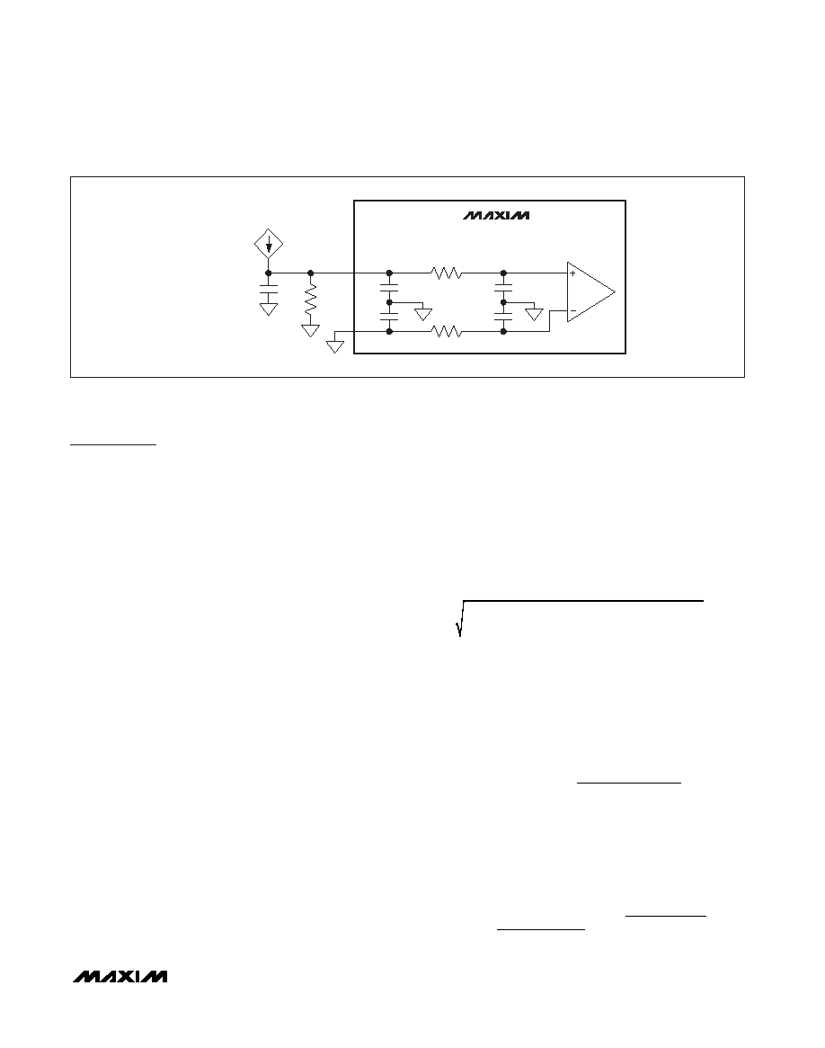
Figure 1 shows the simplified diagram of input imped-
ances for settling time calculations. Sample time is
divided into two parts:
1) tIST: Internal settling time (max 250ns). During this
time, voltage VIN (VINP - VINN) rises with a time con-
stant of:
RIN x (CIN + CPAR)
2) tRC: During this period two things happen:
a. Input VIN keeps increasing from its value at tIST
to its final value with a new time constant of:
b. RSW and CS track this VIN (input) with a time con-
stant of RSW x CS, which is 12.5ns (worst case).
Example:
Approximate accuracy calculations can be done for an
input voltage based on the above impedance values.
These calculations can be divided into three parts.
1) Accuracy of input at tIST (250ns):
where t1 = tIST = 250ns.
At tIST the internal circuit tags input impedance.
This causes charge redistribution to occur, which
causes a dip in the input voltage. The worst-case
value of the input voltage at tIST is:
V
C
CC
C
e
IN
t
S
IN
PAR
S
t
IST
@
=
++
()
×
11
R
RC
C
IN
PAR
V
×+
()
×
Accuracy
e
t
RC
C
IN
PAR
=
×+
()
1
RC
C
R
C
IN
PAR
SW
S
×+
()
() +×
()
2
DS1843
CS
CIN
CPAR
CIN
INPUT MODEL
RSW
VINP
VINN
RSW
RIN
CURRENT
MIRROR OUTPUT
Figure 1. Input Impedances for Settling Time Calculations Diagram
相关PDF资料 |
PDF描述 |
|---|---|
| DS21602N+ | IC ADAPTER CLOCK RATE 8-DIP |
| DS21610SN+ | IC ADAPT CLK RATE 3.3V/5V 16SOIC |
| DS2165Q+T&R | IC PROC ADPCM 16/24/32K 28-PLCC |
| DS2450S+T&R | IC CONVERTER A/D QUAD 1-W 8-SOIC |
| DS3508E+ | IC GAMMA BUFFER 8CH 20-TSSOP |
相关代理商/技术参数 |
参数描述 |
|---|---|
| DS1843D TRL | 制造商:MAXIM 制造商全称:Maxim Integrated Products 功能描述:Fast Sample-and-Hold Circuit |
| DS1843D+ | 功能描述:采样&保持放大器 Fast Sample & Hold Circuit RoHS:否 制造商:Texas Instruments 通道数量:2 捕获时间:20 us 电源电压-最大:18 V 最大工作温度:+ 85 C 最小工作温度:- 25 C 安装风格: 封装 / 箱体:SOIC-14 封装:Tube |
| DS1843D+TRL | 功能描述:采样&保持放大器 Fast Sample & Hold Circuit RoHS:否 制造商:Texas Instruments 通道数量:2 捕获时间:20 us 电源电压-最大:18 V 最大工作温度:+ 85 C 最小工作温度:- 25 C 安装风格: 封装 / 箱体:SOIC-14 封装:Tube |
| DS1843K | 功能描述:放大器 IC 开发工具 Fast Sample & Hold Circuit RoHS:否 制造商:International Rectifier 产品:Demonstration Boards 类型:Power Amplifiers 工具用于评估:IR4302 工作电源电压:13 V to 23 V |
| DS1844 | 制造商:DALLAS 制造商全称:Dallas Semiconductor 功能描述:Quad Digital Potentiometer |
发布紧急采购,3分钟左右您将得到回复。