- 您现在的位置:买卖IC网 > PDF目录9050 > DS1854B-050 (Maxim Integrated Products)IC RES TEMP-CNTRL 50/50K 16BGA PDF资料下载
参数资料
| 型号: | DS1854B-050 |
| 厂商: | Maxim Integrated Products |
| 文件页数: | 10/22页 |
| 文件大小: | 0K |
| 描述: | IC RES TEMP-CNTRL 50/50K 16BGA |
| 产品培训模块: | Lead (SnPb) Finish for COTS Obsolescence Mitigation Program |
| 标准包装: | 810 |
| 接片: | 256 |
| 电阻(欧姆): | 50k |
| 电路数: | 2 |
| 温度系数: | 标准值 50 ppm/°C |
| 存储器类型: | 非易失 |
| 接口: | I²C(设备位址) |
| 电源电压: | 3 V ~ 5.5 V |
| 工作温度: | -40°C ~ 95°C |
| 安装类型: | 表面贴装 |
| 封装/外壳: | 16-LBGA,CSPBGA |
| 供应商设备封装: | 16-CSBGA(4x4) |
| 包装: | 托盘 |
DS1854
Dual Temperature-Controlled
Resistors with Two Monitors
18
____________________________________________________________________
Temperature Conversion
The direct-to-digital temperature sensor measures tem-
perature through the use of an on-chip temperature mea-
surement technique with an operating range from
-40°C to +102°C. Temperature conversions are initiated
upon power-up, and the most recent conversion is stored
in memory locations 60h and 61h of the Main Device,
which are updated every tframe. Temperature conver-
sions do not occur during an active read or write to
memory.
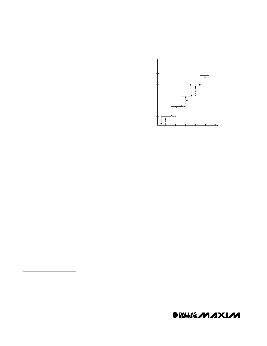
The value of each resistor is determined by the tempera-
ture-addressed look-up table. The look-up table assigns
a unique value to each resistor for every 2°C increment
with a 1°C hysteresis at a temperature transition over the
operating temperature range (see Figure 4).
Power-Up and Low-Voltage Operation
During power-up, the device is inactive until VCC
exceeds the digital power-on-reset voltage (POD). At this
voltage, the digital circuitry, which includes the 2-wire
interface, becomes functional. However, EEPROM
backed registers/settings cannot be internally read
(recalled into shadow SRAM) until VCC exceeds the ana-
log power-on-reset voltage (POA) at which time the
remainder of the device becomes fully functional. Once
VCC exceeds POA, the RDYB bit in byte 6Eh of the Main
Device memory is timed to go from a 1 to a 0 and indi-
cates when analog to digital conversions begin. If VCC
ever dips below POA, the RDYB bit will read as a 1 again.
Once a device exceeds POA and the EEPROM is
recalled, the values remain active (recalled) until VCC falls
below POD.
For 2-wire device addresses sourced from EEPROM
(ADFIX = 1), the device address defaults to A2h until VCC
exceeds POA and the EEPROM values are recalled. The
Auxiliary Device (A0h) is always available within this volt-
age window (between POD and the EEPROM recall)
regardless of the programmed state of ADEN.
Furthermore, as the device powers-up, the VCClo alarm
flag (bit 4 of 70h in Main Device) will default to a 1 until
the first VCC analog-to-digital conversion occurs and sets
or clears the flag accordingly.
2-Wire Operation
Clock and Data Transitions: The SDA pin is normally
pulled high with an external resistor or device. Data on
the SDA pin may only change during SCL-low time
periods. Data changes during SCL-high periods will
indicate a start or stop condition depending on the con-
ditions discussed below. See the timing diagrams in
Figures 5 and 6 for further details.
Start Condition: A high-to-low transition of SDA with
SCL high is a start condition, which must precede any
other command. See the timing diagrams in Figures 5
and 6 for further details.
Stop Condition: A low-to-high transition of SDA with
SCL high is a stop condition. After a read or write
sequence, the stop command places the DS1854 into a
low-power mode. See the timing diagrams in Figures 5
and 6 for further details.
Acknowledge: All address and data bytes are trans-
mitted through a serial protocol. The DS1854 pulls the
SDA line low during the ninth clock pulse to acknowl-
edge that it has received each word.
Standby Mode: The DS1854 features a low-power
mode that is automatically enabled after power-on,
after a stop command, and after the completion of all
internal operations.
Device Addressing: The DS1854 must receive an 8-bit
device address word following a start condition to
enable a specific device for a read or write operation.
The address word is clocked into this part’s MSB to
LSB. The address byte consists of Ah followed by A2h
or the value in Table 01 8Ch for the Main Device, or
A0h for the Auxiliary Device then the R/W bit. This byte
must match the address programmed into Table 01
8Ch or A0h (for the Auxiliary Device). If a device
address match occurs, this part will output a zero for
one clock cycle as an acknowledge and the corre-
sponding block of memory is enabled (see the Memory
Organization section). If the R/W bit is high, a read
operation is initiated. If the R/W is low, a write operation
is initiated (see the Memory Organization section). If
M6
M5
M4
M3
M2
M1
24
6
8
10
12
TEMPERATURE (
°C)
MEMORY
LOCATION
INCREASING
TEMPERATURE
DECREASING
TEMPERATURE
Figure 4. Look-Up Table Memory Hysteresis
相关PDF资料 |
PDF描述 |
|---|---|
| MS3450W32-17PY | CONN RCPT 4POS WALL MNT W/PINS |
| MS3450W32-17PX | CONN RCPT 4POS WALL MNT W/PINS |
| MS3450W32-17PW | CONN RCPT 4POS WALL MNT W/PINS |
| FST3253QSC | MUX/DEMUX DUAL 4:1 TTL 16QSOP |
| VI-J1H-MZ-F1 | CONVERTER MOD DC/DC 52V 25W |
相关代理商/技术参数 |
参数描述 |
|---|---|
| DS1854E-050 | 功能描述:数字电位计 IC RoHS:否 制造商:Maxim Integrated 电阻:200 Ohms 温度系数:35 PPM / C 容差:25 % POT 数量:Dual 每 POT 分接头:256 弧刷存储器:Volatile 缓冲刷: 数字接口:Serial (3-Wire, SPI) 描述/功能:Dual Volatile Low Voltage Linear Taper Digital Potentiometer 工作电源电压:1.7 V to 5.5 V 电源电流:27 uA 最大工作温度:+ 125 C 安装风格:SMD/SMT 封装 / 箱体:TQFN-16 封装:Reel |
| DS1855 | 制造商:DALLAS 制造商全称:Dallas Semiconductor 功能描述:Dual Nonvolatile Digital Potentiometer and Secure Memory |
| DS1855-010+ | 制造商:Maxim Integrated Products 功能描述:DUAL NV POT & MEM 10/10K LEAD FREE - Rail/Tube |
| DS1855B-010 | 功能描述:数字电位计 IC RoHS:否 制造商:Maxim Integrated 电阻:200 Ohms 温度系数:35 PPM / C 容差:25 % POT 数量:Dual 每 POT 分接头:256 弧刷存储器:Volatile 缓冲刷: 数字接口:Serial (3-Wire, SPI) 描述/功能:Dual Volatile Low Voltage Linear Taper Digital Potentiometer 工作电源电压:1.7 V to 5.5 V 电源电流:27 uA 最大工作温度:+ 125 C 安装风格:SMD/SMT 封装 / 箱体:TQFN-16 封装:Reel |
| DS1855B-010/T&R | 制造商:Maxim Integrated Products 功能描述:IC RES TEMP-CNTRL 10/10K 16BGA |
发布紧急采购,3分钟左右您将得到回复。