- 您现在的位置:买卖IC网 > PDF目录9173 > DS1859E-050+T&R (Maxim Integrated Products)IC RES TEMP 50/50K 3MON 16-TSSOP PDF资料下载
参数资料
| 型号: | DS1859E-050+T&R |
| 厂商: | Maxim Integrated Products |
| 文件页数: | 23/28页 |
| 文件大小: | 0K |
| 描述: | IC RES TEMP 50/50K 3MON 16-TSSOP |
| 产品培训模块: | Lead (SnPb) Finish for COTS Obsolescence Mitigation Program |
| 标准包装: | 1,000 |
| 接片: | 256 |
| 电阻(欧姆): | 50k |
| 电路数: | 2 |
| 温度系数: | 标准值 50 ppm/°C |
| 存储器类型: | 非易失 |
| 接口: | I²C(设备位址) |
| 电源电压: | 2.85 V ~ 5.5 V |
| 工作温度: | -40°C ~ 95°C |
| 安装类型: | 表面贴装 |
| 封装/外壳: | 16-TSSOP(0.173",4.40mm 宽) |
| 供应商设备封装: | 16-TSSOP |
| 包装: | 带卷 (TR) |
第1页第2页第3页第4页第5页第6页第7页第8页第9页第10页第11页第12页第13页第14页第15页第16页第17页第18页第19页第20页第21页第22页当前第23页第24页第25页第26页第27页第28页
DS1859
Dual, Temperature-Controlled Resistors with
Internally Calibrated Monitors
4
_____________________________________________________________________
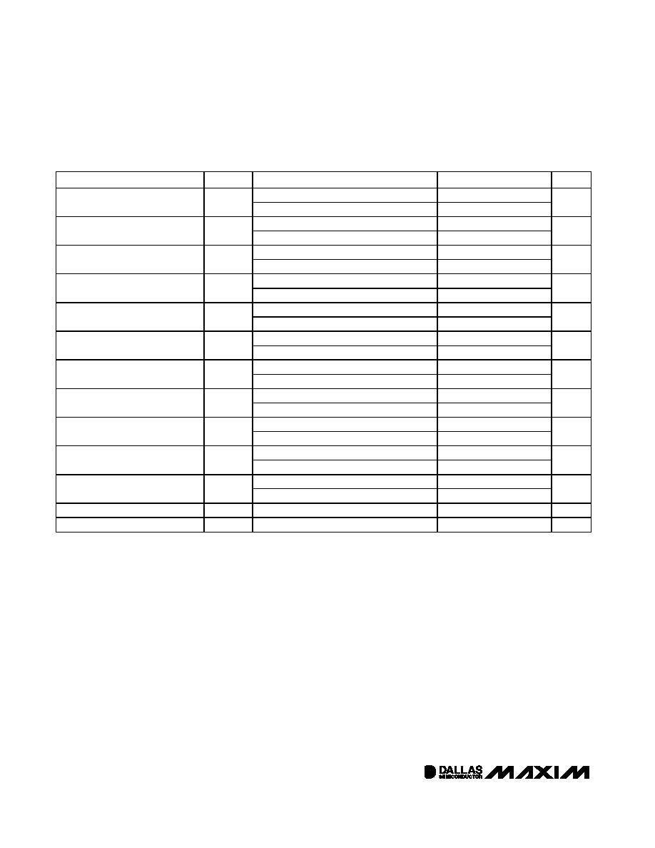
PARAMETER
SYMBOL
CONDITIONS
MIN
TYP
MAX
UNITS
Fast mode (Note 9)
0
400
SCL Clock Frequency
fSCL
Standard mode (Note 9)
0
100
kHz
Fast mode (Note 9)
1.3
Bus Free Time Between STOP and
START Condition
tBUF
Standard mode (Note 9)
4.7
s
Fast mode (Notes 9, 10)
0.6
Hold Time (Repeated)
START Condition
tHD:STA
Standard mode (Notes 9, 10)
4.0
s
Fast mode (Note 9)
1.3
LOW Period of SCL Clock
tLOW
Standard mode (Note 9)
4.7
s
Fast mode (Note 9)
0.6
HIGH Period of SCL Clock
tHIGH
Standard mode (Note 9)
4.0
s
Fast mode (Notes 9, 11, 12)
0
0.9
Data Hold Time
tHD:DAT
Standard mode (Notes 9, 11, 12)
0
s
Fast mode (Note 9)
100
Data Setup Time
tSU:DAT
Standard mode (Note 9)
250
ns
Fast mode (Note 9)
0.6
START Setup Time
tSU:STA
Standard mode (Note 9)
4.7
s
Fast mode (Note 13)
20 + 0.1CB
300
Rise Time of Both SDA and SCL
Signals
tR
Standard mode (Note 13)
20 + 0.1CB
1000
ns
Fast mode (Note 13)
20 + 0.1CB
300
Fall Time of Both SDA and SCL
Signals
tF
Standard mode (Note 13)
20 + 0.1CB
300
ns
Fast mode
0.6
Setup Time for STOP Condition
tSU:STO
Standard mode
4.0
s
Capacitive Load for Each Bus Line
CB
(Note 13)
400
pF
EEPROM Write Time
tW
(Note 14)
10
20
ms
AC ELECTRICAL CHARACTERISTICS
(VCC = 2.85V to 5.5V, TA = -40°C to +95°C, unless otherwise noted. See Figure 6.)
Note 1:
All voltages are referenced to ground.
Note 2:
I/O pins of fast-mode devices must not obstruct the SDA and SCL lines if VCC is switched off.
Note 3:
SDA and SCL are connected to VCC and all other input signals are connected to well-defined logic levels.
Note 4:
Full Scale is user programmable. The maximum voltage that the MON inputs read is approximately Full Scale, even if the volt-
age on the inputs is greater than Full Scale.
Note 5:
This voltage defines the maximum range of the analog-to-digital converter voltage, not the maximum VCC voltage.
Note 6:
Absolute linearity is the difference of measured value from expected value at DAC position. The expected value is a
straight line from measured minimum position to measured maximum position.
Note 7:
Relative linearity is the deviation of an LSB DAC setting change vs. the expected LSB change. The expected LSB change
is the slope of the straight line from measured minimum position to measured maximum position.
Note 8:
See the Typical Operating Characteristics.
Note 9:
A fast-mode device can be used in a standard-mode system, but the requirement tSU:DAT > 250ns must then be met. This
is automatically the case if the device does not stretch the LOW period of the SCL signal. If such a device does stretch the
LOW period of the SCL signal, it must output the next data bit to the SDA line tRMAX + tSU:DAT = 1000ns + 250ns = 1250ns
before the SCL line is released.
相关PDF资料 |
PDF描述 |
|---|---|
| MS27473E18A96PB | CONN PLUG 9POS STRAIGHT W/PINS |
| DS1859E-020+T&R | IC RES TEMP 20/20K 3MON 16-TSSOP |
| DS1855E-050+ | IC RES TEMP-CNTRL 10/50K 14TSSOP |
| MS27497T24F29S | CONN RCPT 29POS WALL MNT W/SCKT |
| DS1848B-C50+T&R | IC RES.MEM TEMP 50/10K 16CSBGA |
相关代理商/技术参数 |
参数描述 |
|---|---|
| DS185XK | 功能描述:数字电位计开发工具 RoHS:否 制造商:Arduino 产品:TinkerKit Rotary Potentiometers 工具用于评估:TinkerKit 电阻:4.7 kOhms 工作电源电压:0 V to 5 V |
| DS1861B | 制造商:Maxim Integrated Products 功能描述:CLOSED LOOP LASER CONTROLLER BGA - Trays |
| DS1861B+ | 功能描述:激光驱动器 Closed Loop Laser Control RoHS:否 制造商:Micrel 数据速率:4.25 Gbps 工作电源电压:3 V to 3.6 V 电源电流:80 mA 最大工作温度:+ 85 C 封装 / 箱体:QFN-16 封装:Tube |
| DS1861E | 制造商:Maxim Integrated Products 功能描述:LASER DRVR 1CH 14TSSOP - Rail/Tube |
| DS1861E+ | 功能描述:激光驱动器 Closed Loop Laser Control RoHS:否 制造商:Micrel 数据速率:4.25 Gbps 工作电源电压:3 V to 3.6 V 电源电流:80 mA 最大工作温度:+ 85 C 封装 / 箱体:QFN-16 封装:Tube |
发布紧急采购,3分钟左右您将得到回复。