参数资料
| 型号: | DS1864K |
| 厂商: | Maxim Integrated Products |
| 文件页数: | 2/72页 |
| 文件大小: | 0K |
| 描述: | KIT EVAL FOR DS1864 |
| 产品培训模块: | Lead (SnPb) Finish for COTS Obsolescence Mitigation Program |
| 标准包装: | 1 |
| 主要目的: | 电源管理,专用型:激光控制器 |
| 已用 IC / 零件: | DS1864 |
第1页当前第2页第3页第4页第5页第6页第7页第8页第9页第10页第11页第12页第13页第14页第15页第16页第17页第18页第19页第20页第21页第22页第23页第24页第25页第26页第27页第28页第29页第30页第31页第32页第33页第34页第35页第36页第37页第38页第39页第40页第41页第42页第43页第44页第45页第46页第47页第48页第49页第50页第51页第52页第53页第54页第55页第56页第57页第58页第59页第60页第61页第62页第63页第64页第65页第66页第67页第68页第69页第70页第71页第72页
�� �
�
�SFP� Laser� Controller� and�
�Diagnostic� IC�
�ABSOLUTE� MAXIMUM� RATINGS�
�Voltage� Range� on� V� CC� Relative� to� Ground� ...........-0.5V� to� +6.0V�
�Voltage� Range� on� Inputs� Relative� to� Ground*� .................-0.5V� to�
�(V� CC� +� 0.5V)�
�Voltage� Range� on� DAC� Pins� Relative� to� Ground*............-0.5V� to�
�(V� CC� +� 0.5V)�
�Current� into� DAC� Pins� ...........................................................5mA�
�Operating� Temperature� Range� ...........................-40°C� to� +95°C�
�Programming� Temperature� Range� .........................0°C� to� +70°C�
�Storage� Temperature� Range� .............................-55°C� to� +125°C�
�Soldering� Temperature............See� IPC/J-STD-020� Specification�
�*� Not� to� exceed� 6.0V.�
�Stresses� beyond� those� listed� under� “Absolute� Maximum� Ratings”� may� cause� permanent� damage� to� the� device.� These� are� stress� ratings� only,� and� functional�
�operation� of� the� device� at� these� or� any� other� conditions� beyond� those� indicated� in� the� operational� sections� of� the� specifications� is� not� implied.� Exposure� to�
�absolute� maximum� rating� conditions� for� extended� periods� may� affect� device� reliability.�
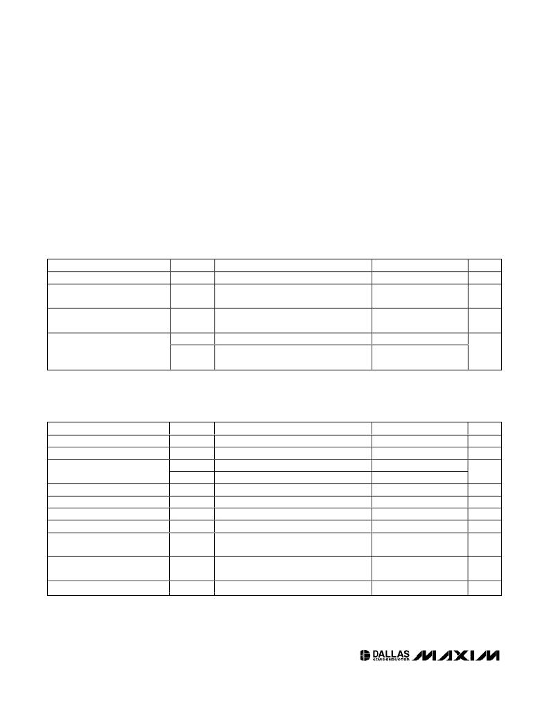
�RECOMMENDED� OPERATING� CONDITIONS�
�(T� A� =� -40°C� to� +95°C)�
�PARAMETER�
�Supply� Voltage�
�Input� Logic� 0� (SDA,� SCL)�
�Input� Logic� 1� (SDA,� SCL)�
�Input� Logic� Levels� (TX-D,� INLOS,�
�RSEL,� IN1)�
�SYMBOL�
�V� CC�
�V� IL�
�V� IH�
�V� IL�
�V� IH�
�CONDITIONS�
�(Note� 1)�
�I� IL� (max)� =� -10μA�
�I� IH� (max)� =� 10μA�
�Input� Logic� 0�
�Input� Logic� 1�
�MIN�
�2.97�
�-0.3�
�0.7� x�
�V� CC�
�-0.3�
�1.5�
�TYP�
�MAX�
�5.50�
�+0.3� x�
�V� CC�
�V� CC� +�
�0.3�
�0.9�
�V� CC� +�
�0.3�
�UNITS�
�V�
�V�
�V�
�V�
�DC� ELECTRICAL� CHARACTERISTICS�
�(V� CC� =� 2.97V� to� 5.5V,� T� A� =� -40°C� to� +95°C.)�
�PARAMETER�
�Supply� Current�
�SYMBOL�
�I� CC�
�CONDITIONS�
�(Notes� 2� and� 3)�
�MIN�
�TYP�
�3�
�MAX�
�5�
�UNITS�
�mA�
�Input� Leakage� (SDA,� SCL)�
�Low-Level� Output� Voltage� (SDA)�
�I/O� Capacitance�
�I� IL�
�V� OL1�
�V� OL2�
�C� I/O�
�3mA� sink� current�
�6mA� sink� current�
�For� SDA/SCL�
�-1�
�+1�
�0.4�
�0.6�
�10�
�μA�
�V�
�pF�
�TX-D� Pullup� Resistor�
�Digital� Power-On� Reset�
�Analog� Power-On� Reset�
�High-Level� Output� Voltage�
�(FETG)�
�Low-Level� Output� Voltage� (TX-F,�
�LOS� Voltage,� FETG)�
�Input� Current� Each� I/O� Pin�
�R� PU�
�V� POD�
�V� POA�
�V� OH�
�V� OL�
�T� A� =� +25°C�
�4mA� source� current�
�4mA� sink� current�
�0.4� <� V� I/O� <� 0.9V� CC�
�14�
�1.0�
�2.00�
�V� CC� -�
�0.4�
�0.0�
�-10�
�20�
�24�
�2.2�
�2.97�
�V� CC� +�
�0.3�
�0.4�
�+10�
�k� ?�
�V�
�V�
�V�
�V�
�μA�
�2�
�_____________________________________________________________________�
�相关PDF资料 |
PDF描述 |
|---|---|
| DS21349DK | KIT DESIGN FOR DS21349 |
| DS21352DK | KIT DESIGN FOR DS21352 |
| DS21354DK | KIT DESIGN FOR DS21354 |
| DS21458DK | KIT DESIGN FOR G511DS21458 |
| DS2156DK | KIT DESIGN FOR DS2156 |
相关代理商/技术参数 |
参数描述 |
|---|---|
| DS1864T | 制造商:Maxim Integrated Products 功能描述:DUAL TMP CTRL DAC+MONITORS,QFN - Rail/Tube |
| DS1864T+ | 功能描述:激光驱动器 SFP Laser Controller & Diagnostic IC RoHS:否 制造商:Micrel 数据速率:4.25 Gbps 工作电源电压:3 V to 3.6 V 电源电流:80 mA 最大工作温度:+ 85 C 封装 / 箱体:QFN-16 封装:Tube |
| DS1864T+T&R | 制造商:Maxim Integrated Products 功能描述:DUAL TMP CTRL DAC+MON QFN T&R LF - Tape and Reel 制造商:Maxim Integrated Products 功能描述:IC LASER CTRLR 1CHAN 5.5V 28TQFN |
| DS1864T+T&R | 功能描述:激光驱动器 SFP Laser Controller & Diagnostic IC RoHS:否 制造商:Micrel 数据速率:4.25 Gbps 工作电源电压:3 V to 3.6 V 电源电流:80 mA 最大工作温度:+ 85 C 封装 / 箱体:QFN-16 封装:Tube |
| DS1865 | 制造商:MAXIM 制造商全称:Maxim Integrated Products 功能描述:PON Triplexer Control and Monitoring Circuit |
发布紧急采购,3分钟左右您将得到回复。