- 您现在的位置:买卖IC网 > PDF目录9174 > DS1868E-50+T&R (Maxim Integrated Products)IC POT DIGITAL DUAL 50K 20-TSSOP PDF资料下载
参数资料
| 型号: | DS1868E-50+T&R |
| 厂商: | Maxim Integrated Products |
| 文件页数: | 3/14页 |
| 文件大小: | 0K |
| 描述: | IC POT DIGITAL DUAL 50K 20-TSSOP |
| 产品培训模块: | Lead (SnPb) Finish for COTS Obsolescence Mitigation Program |
| 标准包装: | 2,500 |
| 接片: | 256 |
| 电阻(欧姆): | 50k |
| 电路数: | 2 |
| 温度系数: | 标准值 750 ppm/°C |
| 存储器类型: | 易失 |
| 接口: | 3 线串口 |
| 电源电压: | 2.7 V ~ 3.3 V,4.5 V ~ 5.5 V |
| 工作温度: | -40°C ~ 85°C |
| 安装类型: | 表面贴装 |
| 封装/外壳: | 20-TSSOP(0.173",4.40mm 宽) |
| 供应商设备封装: | 20-TSSOP |
| 包装: | 带卷 (TR) |
DS1868
11 of 14
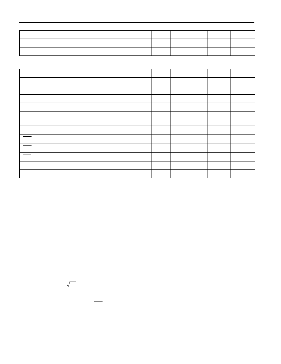
CAPACITANCE
(tA=25
°C)
PARAMETER
SYMBOL
MIN
TYP
MAX
UNITS
NOTES
Input Capacitance
CIN
5
pF
3, 6
Output Capacitance
COUT
7
pF
3, 6
AC ELECTRICAL CHARACTERISTICS
(-40
°C to +85°C; V
CC=5.0V
±10%)
PARAMETER
SYMBOL
MIN
TYP
MAX
UNITS
NOTES
CLK Frequency
fCLK
DC
10
MHz
10
Width of CLK Pulse
tCH
50
ns
10
Data Setup Time
tDC
30
ns
10
Data Hold Time
tCDH
10
ns
10
Propagation Delay Time Low to High Level
Clock to Output
tPLH
50
ns
10, 13
Propagation Delay Time High to Low Level
tPLH
50
ns
10, 13
RST
High to Clock Input High
tCC
50
ns
10
RST
Low from Clock Input High
tHLT
50
ns
10
RST
Inactive
tRLT
125
ns
10
Clock Low to Data Valid on a Read
tCDD
30
ns
10
CLK Rise Time, CLK Fall Time
tCR
50
ns
10
NOTES:
1. All voltages are referenced to ground.
2. Resistor inputs cannot exceed VB - 0.5V in the negative direction.
3. Capacitance values apply at 25
°C.
4. Absolute linearity is used to determine wiper voltage versus expected voltage as determined by wiper
position. Device test limits
±1.6 LSB.
5. Relative linearity is used to determine the change in voltage between successive tap positions. Device
test limits
±0.5 LSB.
6. Typical values are for tA = 25
°C and nominal supply voltage.
7. -3 dB cutoff frequency characteristics for the DS1868 depend on potentiometer total resistance:
DS1868-010; 1 MHz, DS1868-050; 200 kHz; and DS1868-100; 80 kHz.
8. Cout is active regardless of the state of RST .
9. VREF = 1.5 volts.
10. See Figure 9(a), (b), and (c).
11. Noise < -120 dB/ Hz . Reference 1 volt (thermal).
12. Supply current is dependent on clock rate (see Figure 11).
13. See Figure 10.
14. Standby currents apply when RST , LLIC, DQ are in the low-state.
15. When biasing the substrate minimum VB = -3.0V
±10% and maximum V
CC = 3.0V
±10%.
16. Valid at 25
°C only.
相关PDF资料 |
PDF描述 |
|---|---|
| DS1868E-100+T&R | IC POT DIGITAL DUAL 100K 20TSSOP |
| DS1847B-010+T&R | IC RES TEMP-CNTRL 10/10K 16-BGA |
| DS1847B-050+T&R | IC RES TEMP-CNTRL 50/10K 16-BGA |
| MAX5408ETE+ | IC POT DGTL DUAL AUDIO 16-TQFN |
| MAX5410ETE+ | IC POT DGTL DUAL AUDIO 16-TQFN |
相关代理商/技术参数 |
参数描述 |
|---|---|
| DS1868EN-010 | 制造商:未知厂家 制造商全称:未知厂家 功能描述:Digital Potentiometer |
| DS1868EN-050 | 制造商:未知厂家 制造商全称:未知厂家 功能描述:Digital Potentiometer |
| DS1868EN-100 | 制造商:未知厂家 制造商全称:未知厂家 功能描述:Digital Potentiometer |
| DS1868N-010 | 制造商:未知厂家 制造商全称:未知厂家 功能描述:Digital Potentiometer |
| DS1868N-050 | 制造商:未知厂家 制造商全称:未知厂家 功能描述:Digital Potentiometer |
发布紧急采购,3分钟左右您将得到回复。