- 您现在的位置:买卖IC网 > PDF目录9184 > DS1882E-050+T&R (Maxim Integrated Products)IC POT DIGIT DL LOG 50K 16TSSOP PDF资料下载
参数资料
| 型号: | DS1882E-050+T&R |
| 厂商: | Maxim Integrated Products |
| 文件页数: | 4/15页 |
| 文件大小: | 0K |
| 描述: | IC POT DIGIT DL LOG 50K 16TSSOP |
| 产品培训模块: | Lead (SnPb) Finish for COTS Obsolescence Mitigation Program |
| 标准包装: | 1,000 |
| 接片: | 64 |
| 电阻(欧姆): | 45k |
| 电路数: | 2 |
| 温度系数: | 标准值 750 ppm/°C |
| 存储器类型: | 非易失 |
| 接口: | I²C(设备位址) |
| 电源电压: | 4.5 V ~ 7 V |
| 工作温度: | -40°C ~ 85°C |
| 安装类型: | 表面贴装 |
| 封装/外壳: | 16-TSSOP(0.173",4.40mm 宽) |
| 供应商设备封装: | 16-TSSOP |
| 包装: | 带卷 (TR) |
DS1882
Dual Log Audio Digital Potentiometer
12
____________________________________________________________________
Writing Command Byte Values
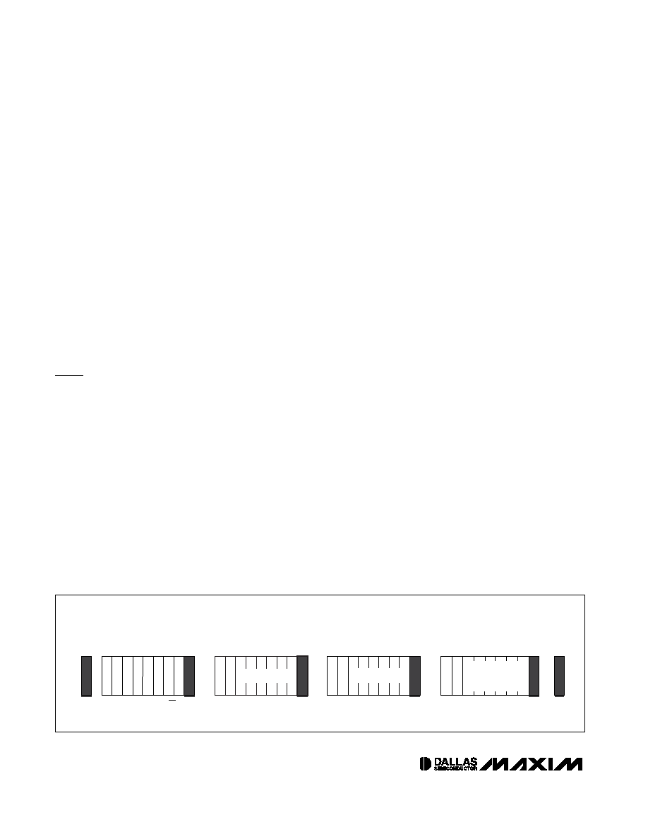
An example of writing to the DS1882 is shown in Figure 2.
The DS1882 has one write command that is used to
change the Potentiometer Wiper Setting Registers and
the Configuration Register. All write operations begin with
a START from the master, followed by a slave address
byte. The R/W bit should be written to 0, which initiates
a write command. Once the slave address byte has
been issued and the master receives the acknowledge
from the DS1882, potentiometer wiper data is transmit-
ted to the DS1882 by the master device.
If the potentiometer has been configured to be written
in nonvolatile memory (see the Configuration Register
section), then the acknowledge needs to be followed
with a STOP command. This command is required from
the master at the end of data transmission to initiate the
EEPROM write. The STOP command is also accepted if
the user has configured the pot values to be written in
volatile memory, but no EEPROM is written to.
I2C Serial Interface Description
I2C interface supports a bidirectional data transmission
protocol with device addressing. A device that sends
data on the bus is defined as a transmitter, and a
device receiving data as a receiver. The device that
controls the message is called a master. The devices
that are controlled by the master are slaves. The bus
must be controlled by a master device that generates
the serial clock (SCL), controls the bus access, and
generates the START and STOP conditions. The
DS1882 operates as a slave on the I2C bus. Connections
to the bus are made by the open-drain I/O lines, SDA
and SCL. The following I/O terminals control the I2C
serial port: CE, SDA, SCL, A0, A1, and A2. A data
transfer protocol and a timing diagram are provided in
Figures 3 and 4. The following terminology is commonly
used to describe I2C data transfers.
I2C Definitions
Master Device: The master device controls the slave
devices on the bus. The master device generates SCL
clock pulses, START and STOP conditions.
Slave Devices: Slave devices send and receive data
at the master’s request.
Bus Idle or Not Busy: Time between STOP and START
conditions when both SDA and SCL are inactive and in
their logic-high states. When the bus is idle it often initi-
ates a low-power mode for slave devices.
START Condition: A START condition is generated by
the master to initiate a new data transfer with a slave.
Transitioning SDA from high to low while SCL remains
high generates a START condition. See the timing dia-
gram for applicable timing.
STOP Condition: A STOP condition is generated by
the master to end a data transfer with a slave.
Transitioning SDA from low to high while SCL remains
high generates a STOP condition. See the timing dia-
gram for applicable timing.
Repeated START Condition: The master can use a
repeated START condition at the end of one data trans-
fer to indicate that it will immediately initiate a new data
transfer following the current one. Repeated STARTs
are commonly used during read operations to identify a
specific memory address to begin a data transfer. A
repeated START condition is issued identically to a nor-
mal START condition. See the timing diagram for
applicable timing.
Bit Write: Transitions of SDA must occur during the low
state of SCL. The data on SDA must remain valid and
unchanged during the entire high pulse of SCL plus the
setup and hold-time requirements (see Figure 4). Data is
shifted into the device during the rising edge of the SCL.
Bit Read: At the end of a write operation, the master
must release the SDA bus line for the proper amount of
WRITE PROTOCOL
0
MSB
LSB
POT-0
1
0
MSB
LSB
POT-1
A
0
A
1
A
2
0
101
0
MSB
LSB
R/W = 0
DATA BYTES CAN BE WRITTEN IN ANY ORDER.
COMMAND
BYTE
COMMAND
BYTE
COMMAND
BYTE
SLAVE ADDRESS
BYTE
MSB
LSB
CONFIG
REG
10
ST
AR
T
ACK
STOP
Figure 2. Write Protocol
相关PDF资料 |
PDF描述 |
|---|---|
| VI-BWZ-MW-F3 | CONVERTER MOD DC/DC 2V 40W |
| VI-B5L-MV | CONVERTER MOD DC/DC 28V 150W |
| DS1805E-010+T&R | IC POT DIG ADDRESS 10K 14-TSSOP |
| VI-BWZ-MW-F2 | CONVERTER MOD DC/DC 2V 40W |
| VI-BWZ-MW-F1 | CONVERTER MOD DC/DC 2V 40W |
相关代理商/技术参数 |
参数描述 |
|---|---|
| DS1882Z-050 | 制造商:Maxim Integrated Products 功能描述:DUAL NV +/-5V AUDIO POT SOIC-16 - Rail/Tube |
| DS1882Z-050/T&R | 制造商:Maxim Integrated Products 功能描述:DUAL NV +/-5V AUDIO POT SOIC16 T& - Tape and Reel |
| DS1882Z-050+ | 功能描述:数字电位计 IC Dual NV Audio Taper RoHS:否 制造商:Maxim Integrated 电阻:200 Ohms 温度系数:35 PPM / C 容差:25 % POT 数量:Dual 每 POT 分接头:256 弧刷存储器:Volatile 缓冲刷: 数字接口:Serial (3-Wire, SPI) 描述/功能:Dual Volatile Low Voltage Linear Taper Digital Potentiometer 工作电源电压:1.7 V to 5.5 V 电源电流:27 uA 最大工作温度:+ 125 C 安装风格:SMD/SMT 封装 / 箱体:TQFN-16 封装:Reel |
| DS1882Z-050+T&R | 制造商:Maxim Integrated Products 功能描述:DGTL POTENTIOMETER 64POS 45KOHM DUAL 16SOIC N - Tape and Reel 制造商:Maxim Integrated Products 功能描述:IC POT DIGIT DL LOG 50K 16SOIC 制造商:Maxim Integrated Products 功能描述:Digital Potentiometer ICs Dual NV Audio Taper |
| DS1882Z-050+T&R | 功能描述:数字电位计 IC Dual NV Audio Taper RoHS:否 制造商:Maxim Integrated 电阻:200 Ohms 温度系数:35 PPM / C 容差:25 % POT 数量:Dual 每 POT 分接头:256 弧刷存储器:Volatile 缓冲刷: 数字接口:Serial (3-Wire, SPI) 描述/功能:Dual Volatile Low Voltage Linear Taper Digital Potentiometer 工作电源电压:1.7 V to 5.5 V 电源电流:27 uA 最大工作温度:+ 125 C 安装风格:SMD/SMT 封装 / 箱体:TQFN-16 封装:Reel |
发布紧急采购,3分钟左右您将得到回复。