- 您现在的位置:买卖IC网 > PDF目录97866 > DS21348T (DALLAS SEMICONDUCTOR) DATACOM, PCM TRANSCEIVER, PQFP44 PDF资料下载
参数资料
| 型号: | DS21348T |
| 厂商: | DALLAS SEMICONDUCTOR |
| 元件分类: | Digital Transmission Interface |
| 英文描述: | DATACOM, PCM TRANSCEIVER, PQFP44 |
| 封装: | TQFP-44 |
| 文件页数: | 5/67页 |
| 文件大小: | 339K |
| 代理商: | DS21348T |
第1页第2页第3页第4页当前第5页第6页第7页第8页第9页第10页第11页第12页第13页第14页第15页第16页第17页第18页第19页第20页第21页第22页第23页第24页第25页第26页第27页第28页第29页第30页第31页第32页第33页第34页第35页第36页第37页第38页第39页第40页第41页第42页第43页第44页第45页第46页第47页第48页第49页第50页第51页第52页第53页第54页第55页第56页第57页第58页第59页第60页第61页第62页第63页第64页第65页第66页第67页
DS21348/Q348
13 of 67
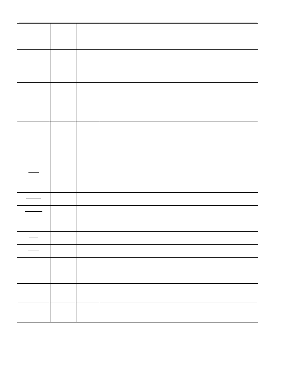
Acronym
Pin
I/O
Description
RD*
(DS*)
2I
Read Input (Data Strobe). RD* and DS* are active low signals.
DS active low when in non-multiplexed, Motorola mode. See the
Bus Timing Diagrams in section 5.
RCL/
LOTC
25
O
Receive Carrier Loss / Loss of Transmit Clock. An output which
will toggle high during a receive carrier loss (CCR2.7 = 0) or will
toggle high if the TCLK pin has not been toggled for 5
sec ± 2
sec (CCR2.7 = 1). CCR2.7 defaults to logic 0 when in hardware
mode.
RNEG
39
O
Receive Negative Data. Updated on the rising edge (CCR2.0 = 0)
or the falling edge (CCR2.0 = 1) of RCLK with the bipolar data out
of the line interface. Set NRZE (CCR1.6) to a one for NRZ
applications. In NRZ mode, data will be output on RPOS while a
received error will cause a positive-going pulse synchronous with
RCLK at RNEG. See section 8.4 for details.
RPOS
38
O
Receive Positive Data. Updated on the rising edge (CCR2.0 = 0) or
the falling edge (CCR2.0 = 1) of RCLK with bipolar data out of the
line interface. Set NRZE (CCR1.6) to a one for NRZ applications.
In NRZ mode, data will be output on RPOS while a received error
will cause a positive-going pulse synchronous with RCLK at RNEG.
See section 8.4 for details.
RT0/
RT1
44/
23
I
Receive LIU Termination Select Bits 0 & 1 [H/W Mode]. These
inputs determine the receive termination. See Table 4-8.
RTIP/
RRING
27/
28
I
Receive Tip and Ring. Analog inputs for clock recovery circuitry.
These pins connect via a 1:1 transformer to the line. See Section 7
for details.
SCLK
5I
Serial Clock. Serial bus clock input.
SCLKE
4I
Receive & Transmit Synchronization Clock Enable. SCLKE
combines RSCLKE (CCR5.3) and TSCLKE (CCR5.2).
0 = disable 2.048 MHz synchronization transmit and receive mode
1 = enable 2.048 MHz synchronization transmit and receive mode
SDI
6I
Serial Data Input. Sampled on rising edge (ICES = 0) or the
falling edge (ICES = 1) of SCLK.
SDO
7O
Serial Data Output. Valid on the falling edge (OCES = 0) or the
rising edge (OCES = 1) of SCLK.
TCLK
43
I
Transmit Clock. A 2.048 MHz or 1.544 MHz primary clock. Used
to clock data through the transmit side formatter. Can be sourced
internally by MCLK or RCLK. See Common Control Register 1
and Figure 3-3.
TEST
26
I
3-State Control. Set high to tri-state all outputs and I/O pins
(including the parallel control port). Set low for normal operation.
Useful in board level testing.
TNEG
42
I
Transmit Negative Data. Sampled on the falling edge (CCR2.1 =
0) or the rising edge (CCR2.1 = 1) of TCLK for data to be
transmitted out onto the line.
相关PDF资料 |
PDF描述 |
|---|---|
| DS21348TN | DATACOM, PCM TRANSCEIVER, PQFP44 |
| DS21348G | DATACOM, PCM TRANSCEIVER, BGA49 |
| DS21Q348N | DATACOM, PCM TRANSCEIVER, PBGA144 |
| DS21Q348 | DATACOM, PCM TRANSCEIVER, PBGA144 |
| DS21352L | DATACOM, PCM TRANSCEIVER, PQFP100 |
相关代理商/技术参数 |
参数描述 |
|---|---|
| DS21348T+ | 功能描述:网络控制器与处理器 IC 3.3V E1/T1/J1 Line Interface RoHS:否 制造商:Micrel 产品:Controller Area Network (CAN) 收发器数量: 数据速率: 电源电流(最大值):595 mA 最大工作温度:+ 85 C 安装风格:SMD/SMT 封装 / 箱体:PBGA-400 封装:Tray |
| DS21348TB | 功能描述:网络控制器与处理器 IC RoHS:否 制造商:Micrel 产品:Controller Area Network (CAN) 收发器数量: 数据速率: 电源电流(最大值):595 mA 最大工作温度:+ 85 C 安装风格:SMD/SMT 封装 / 箱体:PBGA-400 封装:Tray |
| DS21348TN | 功能描述:网络控制器与处理器 IC 3.3V E1/T1/J1 Line Interface RoHS:否 制造商:Micrel 产品:Controller Area Network (CAN) 收发器数量: 数据速率: 电源电流(最大值):595 mA 最大工作温度:+ 85 C 安装风格:SMD/SMT 封装 / 箱体:PBGA-400 封装:Tray |
| DS21348TN+ | 功能描述:网络控制器与处理器 IC 3.3V E1/T1/J1 Line Interface RoHS:否 制造商:Micrel 产品:Controller Area Network (CAN) 收发器数量: 数据速率: 电源电流(最大值):595 mA 最大工作温度:+ 85 C 安装风格:SMD/SMT 封装 / 箱体:PBGA-400 封装:Tray |
| DS21348TNB | 功能描述:网络控制器与处理器 IC RoHS:否 制造商:Micrel 产品:Controller Area Network (CAN) 收发器数量: 数据速率: 电源电流(最大值):595 mA 最大工作温度:+ 85 C 安装风格:SMD/SMT 封装 / 箱体:PBGA-400 封装:Tray |
发布紧急采购,3分钟左右您将得到回复。