- 您现在的位置:买卖IC网 > PDF目录378591 > DS21Q58 (Maxim Integrated Products, Inc.) Dallas Semiconductor PDF资料下载
参数资料
| 型号: | DS21Q58 |
| 厂商: | Maxim Integrated Products, Inc. |
| 英文描述: | Dallas Semiconductor |
| 中文描述: | E1四收发器 |
| 文件页数: | 14/74页 |
| 文件大小: | 647K |
| 代理商: | DS21Q58 |
第1页第2页第3页第4页第5页第6页第7页第8页第9页第10页第11页第12页第13页当前第14页第15页第16页第17页第18页第19页第20页第21页第22页第23页第24页第25页第26页第27页第28页第29页第30页第31页第32页第33页第34页第35页第36页第37页第38页第39页第40页第41页第42页第43页第44页第45页第46页第47页第48页第49页第50页第51页第52页第53页第54页第55页第56页第57页第58页第59页第60页第61页第62页第63页第64页第65页第66页第67页第68页第69页第70页第71页第72页第73页第74页
DS21Q58 E1 Quad Transceiver
14 of 74
6. HOST INTERFACE PORT
The DS21Q58 is controlled through either a nonmultiplexed bus, a multiplexed bus, or serial interface bus by an
external microcontroller or microprocessor. The device can operate with either Intel or Motorola bus timing
configurations. See
Table 6-1
for a description of the bus configurations. Motorola bus signals are listed in
parentheses (). See the timing diagrams in the
AC Electrical Characteristics
in Section
26
for more details.
Table 6-1. Bus Mode Select
PBTS
0
0
1
1
X
X
BTS1
0
0
0
0
1
1
BTS0
0
1
0
1
0
1
PARALLEL PORT MODE
Intel Multiplexed
Intel Nonmultiplexed
Motorola Multiplexed
Motorola Nonmultiplexed
Serial
TEST (Outputs High-Z)
6.1 Parallel Port Operation
When using the parallel interface on the DS21Q58 (BTS1 = 0) the user has the option for either multiplexed bus
operation (BTS1 = 0, BTS0 = 0) or nonmultiplexed bus operation (BTS1 = 0, BTS0 = 1). The DS21Q58 can operate
with either Intel or Motorola bus timing configurations. If the PBTS pin is wired low, Intel timing is selected; if wired
high, Motorola timing is selected. All Motorola bus signals are listed in parentheses (). See the timing diagrams in
Section
26
for more details.
6.2 Serial Port Operation
Setting the BTS1 pin = 1 and BTS0 pin = 0 enables the serial bus interface on the DS21Q58. Port read/write timing
is unrelated to the system transmit and receive timing, allowing asynchronous reads or writes by the host. See
Section
26
for the AC timing of the serial port. All serial port accesses are LSB first. See
Figure 6-1
,
Figure 6-2
,
Figure 6-3
, and
Figure 6-4
for more details.
Reading or writing to the internal registers requires writing one address/command byte prior to transferring register
data. The first bit written (LSB) of the address/command byte specifies whether the access is a read (1) or a write
(0). The next five bits identify the register address. The next bit is reserved and must be set to 0 for proper
operation. The last bit (MSB) of the address/command byte enables the burst mode when set to 1. The burst mode
causes all registers to be consecutively written or read.
All data transfers are initiated by driving the
CS
input low. When input-clock edge select (ICES) is low, input data is
latched on the rising edge of SCLK; when ICES is high, input data is latched on the falling edge of SCLK. When
output-clock edge select (OCES) is low, data is output on the falling edge of SCLK; when OCES is high, data is
output on the rising edge of SCLK. Data is held until the next falling or rising edge. All data transfers are terminated
if the
CS
input transitions high. Port control logic is disabled and SDO is tri-stated when
CS
is high.
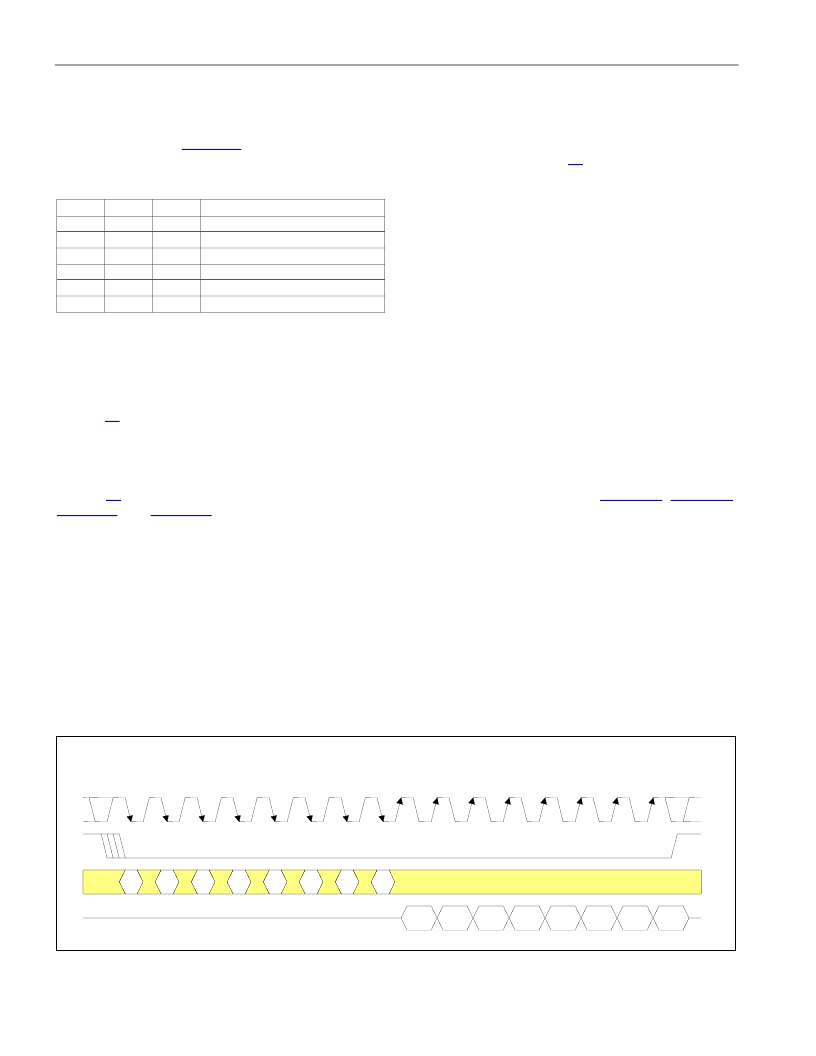
Figure 6-1. Serial Port Operation Mode 1
ICES = 1 (SAMPLE SDI ON THE FALLING EDGE OF SCLK)
OCES = 1 (UPDATE SDO ON THE RISING EDGE OF SCLK)
1
2
3
4
5
6
7
8
9
10
11
12
13
14
15
16
R/
W
A0
A1
A2
A3
A4
A5
B
D1
D2
D3
D4
D5
D6
SCLK
SDI
SDO
CS
LSB
MSB
D0
LSB
D7
MSB
相关PDF资料 |
PDF描述 |
|---|---|
| DS2227-70 | Flexible NV SRAM Stik |
| DS2227-100 | Flexible NV SRAM Stik |
| DS2227-120 | Flexible NV SRAM Stik |
| DS2227 | Flexible NV SRAM Stik |
| DS2229 | Word-Wide 8 Meg SRAM Stik |
相关代理商/技术参数 |
参数描述 |
|---|---|
| DS21Q58L | 功能描述:网络控制器与处理器 IC Quad E1 Transceiver RoHS:否 制造商:Micrel 产品:Controller Area Network (CAN) 收发器数量: 数据速率: 电源电流(最大值):595 mA 最大工作温度:+ 85 C 安装风格:SMD/SMT 封装 / 箱体:PBGA-400 封装:Tray |
| DS21Q58L+ | 功能描述:网络控制器与处理器 IC Quad E1 Transceiver RoHS:否 制造商:Micrel 产品:Controller Area Network (CAN) 收发器数量: 数据速率: 电源电流(最大值):595 mA 最大工作温度:+ 85 C 安装风格:SMD/SMT 封装 / 箱体:PBGA-400 封装:Tray |
| DS21Q58LN | 功能描述:网络控制器与处理器 IC RoHS:否 制造商:Micrel 产品:Controller Area Network (CAN) 收发器数量: 数据速率: 电源电流(最大值):595 mA 最大工作温度:+ 85 C 安装风格:SMD/SMT 封装 / 箱体:PBGA-400 封装:Tray |
| DS21Q58LN+ | 功能描述:网络控制器与处理器 IC Quad E1 Transceiver RoHS:否 制造商:Micrel 产品:Controller Area Network (CAN) 收发器数量: 数据速率: 电源电流(最大值):595 mA 最大工作温度:+ 85 C 安装风格:SMD/SMT 封装 / 箱体:PBGA-400 封装:Tray |
| DS21Q59 | 制造商:MAXIM 制造商全称:Maxim Integrated Products 功能描述:RELIABILITY REPORT FOR DS21Q59, REV A2 |
发布紧急采购,3分钟左右您将得到回复。