- 您现在的位置:买卖IC网 > PDF目录10985 > DS21Q59L (Maxim Integrated Products)IC TXRX E1 QUAD 3.3V 100-LQFP PDF资料下载
参数资料
| 型号: | DS21Q59L |
| 厂商: | Maxim Integrated Products |
| 文件页数: | 5/76页 |
| 文件大小: | 0K |
| 描述: | IC TXRX E1 QUAD 3.3V 100-LQFP |
| 产品培训模块: | Lead (SnPb) Finish for COTS |
| 产品变化通告: | Product Discontinuation 20/Feb/2012 |
| 标准包装: | 90 |
| 功能: | 收发器 |
| 接口: | E1 |
| 电路数: | 4 |
| 电源电压: | 3.14 V ~ 3.47 V |
| 电流 - 电源: | 230mA |
| 工作温度: | 0°C ~ 70°C |
| 安装类型: | 表面贴装 |
| 封装/外壳: | 100-LQFP |
| 供应商设备封装: | 100-LQFP(14x14) |
| 包装: | 托盘 |
| 包括: | AIS 警报检测器和发生器,回送功能,PRBS 发生器 / 检测器,远程检测器和发生器 |
第1页第2页第3页第4页当前第5页第6页第7页第8页第9页第10页第11页第12页第13页第14页第15页第16页第17页第18页第19页第20页第21页第22页第23页第24页第25页第26页第27页第28页第29页第30页第31页第32页第33页第34页第35页第36页第37页第38页第39页第40页第41页第42页第43页第44页第45页第46页第47页第48页第49页第50页第51页第52页第53页第54页第55页第56页第57页第58页第59页第60页第61页第62页第63页第64页第65页第66页第67页第68页第69页第70页第71页第72页第73页第74页第75页第76页
DS21Q59 Quad E1 Transceiver
13 of 76
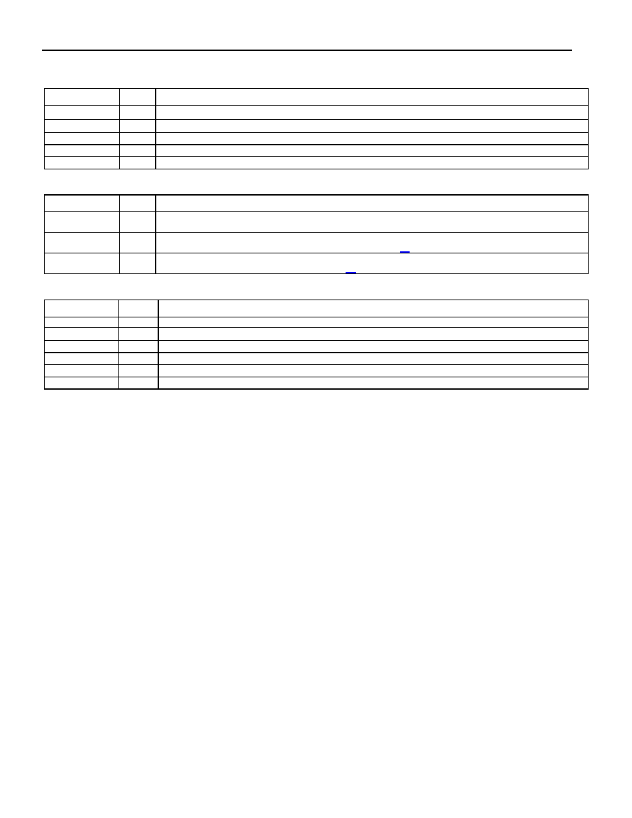
Table 4-G. Serial Port Control Pins
NAME
TYPE
FUNCTION
SDO
O
Serial Port Data Output. Data at this output can be updated on the rising or falling edge of SCLK.
SDI
I
Serial Port Data Input. Data at this input can be sampled on the rising or falling edge of SCLK.
ICES
I
Input Clock-Edge Select. ICES is used to select which SCLK clock edge samples data at SDI.
OCES
I
Output Clock-Edge Select. OCES is used to select which SCLK clock edge updates data at SDO.
SCLK
I
Serial Port Clock. SCLK is used to clock data into and out of the serial port.
Table 4-H. Line Interface Pins
NAME
TYPE
FUNCTION
MCLK
I
Master Clock Input. A 2.048MHz (±50ppm) clock source with TTL levels is applied at this pin. This clock is
used internally for both clock/data recovery and for jitter attenuation.
RTIP and
RRING
I
Receive Tip and Ring. RTIP and RRING are analog inputs for clock recovery circuitry. These pins connect
through a 1:1 step-up transformer to the E1 line. See Section 21 for details.
TTIP and
TRING
O
Transmit Tip and Ring. TTIP and TRING are analog line-driver outputs. These pins connect through a 1:2
step-up transformer to the E1 line. See Section 21 for details.
Table 4-I. Supply Pins
NAME
TYPE
FUNCTION
DVDD
Supply
Digital Positive Supply. 3.3V ±5%. Should be wired to the RVDD and TVDD pins.
RVDD
Supply
Receive Analog Positive Supply. 3.3V ±5%. Should be wired to the DVDD and TVDD pins.
TVDD
Supply
Transmit Analog Positive Supply. 3.3V ±5%. Should be wired to the RVDD and DVDD pins.
DVSS
Supply
Digital Signal Ground. 0V. Should be wired to the RVSS and TVSS pins.
RVSS
Supply
Receive Analog Signal Ground. 0V. Should be wired to DVSS and TVSS.
TVSS
Supply
Transmit Analog Signal Ground. 0V. Should be wired to DVSS and RVSS.
5. FUNCTIONAL DESCRIPTION
The analog AMI/HDB3 waveform off the E1 line is transformer-coupled into the DS21Q59’s RRING and RTIP pins.
The device recovers clock and data from the analog signal and passes it through the jitter attenuation mux to the
receive framer, where the digital serial stream is analyzed to locate the framing/multiframe pattern. The DS21Q59
contains an active filter that reconstructs the analog-received signal for the nonlinear losses that occur in
transmission. The device has a usable receive sensitivity of 0dB to -43dB, which allows the device to operate on
cables over 2km in length. The receive framer locates FAS frame and CRC and CAS multiframe boundaries as well
as detects incoming alarms including carrier loss, loss of synchronization, AIS, and remote alarm. If needed, the
receive elastic store can be enabled to absorb the phase and frequency differences between the recovered E1
data stream and an asynchronous backplane clock, which is provided at the SYSCLK input. The clock applied at
the SYSCLK input can be either a 2.048MHz/4.096MHz/8.192MHz or 16.384MHz clock. The transmit framer is
independent of the receive framer in both the clock requirements and characteristics. The transmit formatter
provides the necessary frame/multiframe data overhead for E1 transmission.
Note: This data sheet assumes a particular nomenclature of the E1 operating environment. In each 125
ms frame,
there are 32 8-bit time slots numbered 0 to 31. Time slot 0 is transmitted first and received first. These 32 time slots
are also referred to as channels with a numbering scheme of 1 to 32. Time slot 0 is identical to channel 1, time slot
1 is identical to channel 2, and so on. Each time slot (or channel) is made up of eight bits that are numbered 1 to 8.
Bit number 1, MSB, is transmitted first. Bit number 8, the LSB, is transmitted last. The term “locked” is used to refer
to two clock signals that are phase-locked or frequency-locked or derived from a common clock (i.e., an 8.192MHz
clock can be locked to a 2.048MHz clock if they share the same 8kHz component).
相关PDF资料 |
PDF描述 |
|---|---|
| VI-B5Z-IX-F2 | CONVERTER MOD DC/DC 2V 30W |
| VI-B5Y-IY-F3 | CONVERTER MOD DC/DC 3.3V 33W |
| VI-B5Y-IX-F1 | CONVERTER MOD DC/DC 3.3V 49.5W |
| VI-B5Y-IW-F4 | CONVERTER MOD DC/DC 3.3V 66W |
| DS2187S/T&R | IC RECEIVE LINE INTERFACE 20SOIC |
相关代理商/技术参数 |
参数描述 |
|---|---|
| DS21Q59L+ | 功能描述:网络控制器与处理器 IC Quad E1 Transceiver RoHS:否 制造商:Micrel 产品:Controller Area Network (CAN) 收发器数量: 数据速率: 电源电流(最大值):595 mA 最大工作温度:+ 85 C 安装风格:SMD/SMT 封装 / 箱体:PBGA-400 封装:Tray |
| DS21Q59LN | 功能描述:网络控制器与处理器 IC Quad E1 Transceiver RoHS:否 制造商:Micrel 产品:Controller Area Network (CAN) 收发器数量: 数据速率: 电源电流(最大值):595 mA 最大工作温度:+ 85 C 安装风格:SMD/SMT 封装 / 箱体:PBGA-400 封装:Tray |
| DS21Q59LN+ | 功能描述:网络控制器与处理器 IC Quad E1 Transceiver RoHS:否 制造商:Micrel 产品:Controller Area Network (CAN) 收发器数量: 数据速率: 电源电流(最大值):595 mA 最大工作温度:+ 85 C 安装风格:SMD/SMT 封装 / 箱体:PBGA-400 封装:Tray |
| DS21S07A | 制造商:Maxim Integrated Products 功能描述: |
| DS21S07AE | 功能描述:SCSI 接口集成电路 RoHS:否 制造商:Texas Instruments 工作电源电压:2.7 V to 5.25 V 电源电流:13 mA 最大工作温度:+ 70 C 最小工作温度:0 C 安装风格:SMD/SMT 封装 / 箱体:SSOP-36 封装:Tube |
发布紧急采购,3分钟左右您将得到回复。