- 您现在的位置:买卖IC网 > PDF目录97868 > DS2404S-001 (MAXIM INTEGRATED PRODUCTS INC) 0 TIMER(S), REAL TIME CLOCK, PDSO16 PDF资料下载
参数资料
| 型号: | DS2404S-001 |
| 厂商: | MAXIM INTEGRATED PRODUCTS INC |
| 元件分类: | Timer or RTC |
| 英文描述: | 0 TIMER(S), REAL TIME CLOCK, PDSO16 |
| 封装: | 0.300 INCH, SOIC-16 |
| 文件页数: | 31/31页 |
| 文件大小: | 1591K |
| 代理商: | DS2404S-001 |
第1页第2页第3页第4页第5页第6页第7页第8页第9页第10页第11页第12页第13页第14页第15页第16页第17页第18页第19页第20页第21页第22页第23页第24页第25页第26页第27页第28页第29页第30页当前第31页
DS2404
9 of 29
The third register (E/S) is a read only register. The first five bits (E4: E0) of this register are called the
ending offset. The ending offset is a byte offset within a page. Bit 5 (PF) is the partial byte flag. Bit 6
(OF) is the overflow flag. Bit 7 (AA) is the authorization accepted flag.
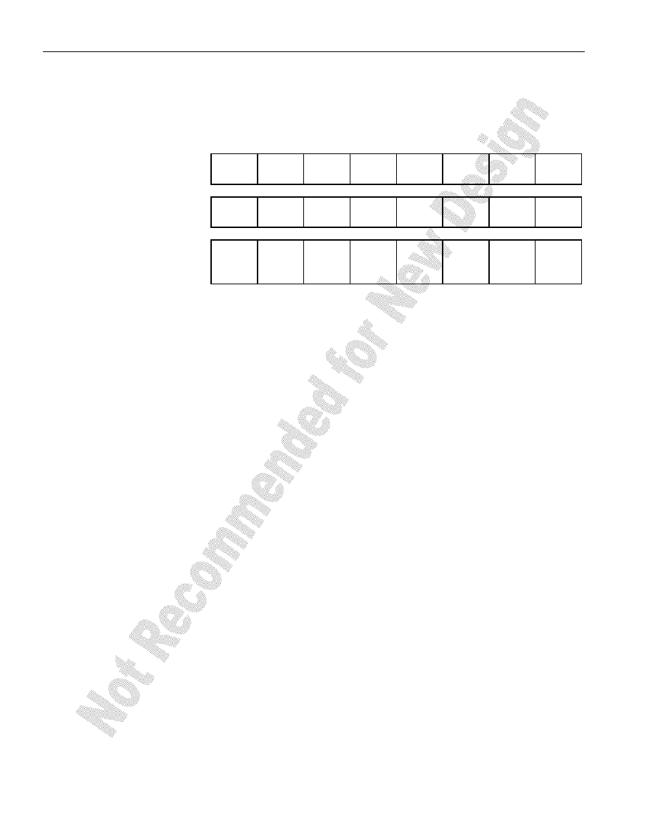
ADDRESS REGISTERS Figure 5
7
6
5
4
3
2
1
0
TARGET ADDRESS (TA1)
T7
T6
T5
T4
T3
T2
T1
T0
TARGET ADDRESS (TA2)
T15
T14
T13
T12
T11
T10
T9
T8
ENDING ADDRESS WITH
DATA STATUS (E/S)
(READ ONLY)
AA
OF
PF
E4
E3
E2
E1
E0
Write Scratchpad Command [0Fh]
After issuing the write scratchpad command, the user must first provide the 2–byte target address,
followed by the data to be written to the scratchpad. The data will be written to the scratchpad starting at
the byte offset (T4:T0). The ending offset (E4: E0) will be the byte offset at which the host stops writing
data. The maximum ending offset is 11111b (31d). If the host attempts to write data past this maximum
offset, the overflow flag (OF) will be set and the remaining data will be ignored. If the user writes an
incomplete byte and an overflow has not occurred, the partial byte flag (PF) will be set.
Read Scratchpad Command [AAh]
This command may be used to verify scratchpad data and target address. After issuing the read scratchpad
command, the user may begin reading. The first two bytes will be the target address. The next byte will
be the ending offset/data status byte (E/S) followed by the scratchpad data beginning at the byte offset
(T4: T0). The user may read data until the end of the scratchpad after which the data read will be all logic
1’s.
Copy Scratchpad [55h]
This command is used to copy data from the scratchpad to memory. After issuing the copy scratchpad
command, the user must provide a 3-byte authorization pattern. This pattern must exactly match the data
contained in the three address registers (TA1, TA2, E/S, in that order). If the pattern matches, the AA
(Authorization Accepted) flag will be set and the copy will begin. At this point, the part will go into a TX
mode, transmitting a logic 1 to indicate the copy is in progress. A logic 0 will be transmitted after the data
has been copied. Any attempt to reset the part will be ignored while the copy is in progress. Copy
typically takes 30
μs.
The data to be copied is determined by the three address registers. The scratchpad data from the
beginning offset through the ending offset, will be copied to memory, starting at the target address.
Anywhere from 1 to 32 bytes may be copied to memory with this command. Whole bytes are copied even
if only partially written. The AA flag will be cleared only by executing a write scratchpad command.
相关PDF资料 |
PDF描述 |
|---|---|
| DS2404B | 0 TIMER(S), REAL TIME CLOCK, PDSO16 |
| DS2404 | 0 TIMER(S), REAL TIME CLOCK, PDIP16 |
| DS2405P | SPECIALTY MEMORY CIRCUIT, PDSO6 |
| DS2405 | SPECIALTY MEMORY CIRCUIT, PBCY3 |
| DS2405Z | SPECIALTY MEMORY CIRCUIT, PDSO4 |
相关代理商/技术参数 |
参数描述 |
|---|---|
| DS2404S-001/T&R | 制造商:Maxim Integrated Products 功能描述:ECONORAM/TIME, SOIC16-TRL (GENERIC) - Tape and Reel |
| DS2404S-001+ | 制造商:Maxim Integrated Products 功能描述:REAL TIME CLOCK SERL 512BYTE 16SOIC - Rail/Tube |
| DS2404S-001+T&R | 制造商:Maxim Integrated Products 功能描述:REAL TIME CLOCK SERL 512BYTE 16SOIC - Tape and Reel |
| DS2404S-C01 | 制造商:未知厂家 制造商全称:未知厂家 功能描述:Peripheral IC |
| DS2405 | 功能描述:接口 - 专用 RoHS:否 制造商:Texas Instruments 产品类型:1080p60 Image Sensor Receiver 工作电源电压:1.8 V 电源电流:89 mA 最大功率耗散: 最大工作温度:+ 85 C 安装风格:SMD/SMT 封装 / 箱体:BGA-59 |
发布紧急采购,3分钟左右您将得到回复。