- 您现在的位置:买卖IC网 > PDF目录11789 > DS2406P+ (Maxim Integrated Products)IC SW ADDRESS DL W/1K MEM 6-TSOC PDF资料下载
参数资料
| 型号: | DS2406P+ |
| 厂商: | Maxim Integrated Products |
| 文件页数: | 24/32页 |
| 文件大小: | 0K |
| 描述: | IC SW ADDRESS DL W/1K MEM 6-TSOC |
| 产品培训模块: | 1-Wire Communications Lead (SnPb) Finish for COTS Obsolescence Mitigation Program |
| 标准包装: | 120 |
| 应用: | 遥控,遥测 |
| 接口: | 1 线 |
| 电源电压: | 2.8 V ~ 6 V |
| 封装/外壳: | 6-LSOJ |
| 供应商设备封装: | 6-TSOC |
| 包装: | 管件 |
| 安装类型: | 表面贴装 |
| 产品目录页面: | 1429 (CN2011-ZH PDF) |
第1页第2页第3页第4页第5页第6页第7页第8页第9页第10页第11页第12页第13页第14页第15页第16页第17页第18页第19页第20页第21页第22页第23页当前第24页第25页第26页第27页第28页第29页第30页第31页第32页
DS2406
30 of 32
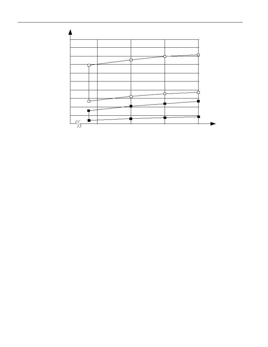
PIO SINK CURRENT
10 mA
20 mA
30 mA
40 mA
50 mA
60 mA
70 mA
80 mA
90 mA
100 mA
I SA , I SB
@ 0.4V
VPUP
PIO-B
max.
min.
PIO-A
max.
min.
4V
5V
6V
2.8V
NOTE: The sink current is production-tested at VPUP = 2.8V; the specification for VPUP of 4V, 5V and
6V is guaranteed by design.
NOTES:
1. All voltages are referenced to ground.
2. VPUP, VPUPA, VPUPB = external pull-up voltage.
3. VIH is a function of the chip-internal supply voltage. This voltage is determined by either the external
pull-up resistor and VPUP or the VCC supply, whichever is higher. Without VCC supply, VIH for either
PIO pin should always be greater than or equal to VPUP -0.3V.
4. Input load is to ground.
5. Leakage current is to ground.
6. Guaranteed by design, not production tested.
7. If the current at PIO-A reaches 200mA the gate voltage of the output transistor will be reduced to
limit the sink current to 200mA. The user-supplied circuitry should limit the current flow through the
PIO-transistor to no more than 100mA. Otherwise the DS2406 may be damaged.
8. PIO-A has a controlled turn-on output. The indicated currents are DC values. At VPUP = 4.0V or
higher the sink current typically reaches 80% of its DC value 1 s after turning on the transistor.
9. VCC must be at least 4.0V if it is to be connected during a programming pulse.
10. Capacitance on the data pin could be 800pF when power is first applied. If a 5k
Ω resistor is used to
pull up the data line to VPUP, 5s after power has been applied the parasite capacitance will not affect
normal communications.
11. The duration of the low pulse sent by the master should be a minimum of 2s with a maximum value
as short as possible to allow time for the pull-up resistor to recover the line to a high level before the
1-Wire device samples in the case of a Write 1 Low Time, or before the master samples in the case of
a Read Low Time.
12. The optimal sampling point for the master is as close as possible to the end time of the 15
μs tRDV
period without exceeding tRDV. For the case of a Read-one time slot, this maximizes the amount of
time for the pull-up resistor to recover the line to a high level. For a Read-zero time slot it ensures
that a read will occur before the fastest 1-Wire devices(s) release the line (tRELEASE = 0).
相关PDF资料 |
PDF描述 |
|---|---|
| VI-BTK-IW-F1 | CONVERTER MOD DC/DC 40V 100W |
| MAX7349AEG+ | IC CNTRL SW SOUND 24-QSOP |
| VI-BTJ-IX-F4 | CONVERTER MOD DC/DC 36V 75W |
| VI-BTJ-IX-F3 | CONVERTER MOD DC/DC 36V 75W |
| VI-BTJ-IX-F1 | CONVERTER MOD DC/DC 36V 75W |
相关代理商/技术参数 |
参数描述 |
|---|---|
| DS2406P/R | 制造商:DALLAS 制造商全称:Dallas Semiconductor 功能描述:Dual Addressable Switch Plus 1kbit Memory |
| DS2406P/T | 制造商:DALLAS 制造商全称:Dallas Semiconductor 功能描述:Dual Addressable Switch Plus 1kbit Memory |
| DS2406P/T&R | 制造商:Maxim Integrated Products 功能描述:IC SW DL ADDRESS W/1K MEM 6-TSOC |
| DS2406P/T&R | 功能描述:接口 - 专用 RoHS:否 制造商:Texas Instruments 产品类型:1080p60 Image Sensor Receiver 工作电源电压:1.8 V 电源电流:89 mA 最大功率耗散: 最大工作温度:+ 85 C 安装风格:SMD/SMT 封装 / 箱体:BGA-59 |
| DS2406P/TR | 制造商:未知厂家 制造商全称:未知厂家 功能描述:Peripheral IC |
发布紧急采购,3分钟左右您将得到回复。